


PCB Assembly
Printed circuit board (PCB) assembly represents a critical phase in electronics manufacturing, where components are mounted onto a board to create functional circuits. This process bridges design and production, ensuring that electronic devices perform reliably in diverse applications. From soldering techniques to component placement, PCB assembly encompasses the methods and technologies that transform bare boards into operational systems. Understanding these elements is essential for engineers, hobbyists, and industry professionals aiming to optimize production efficiency and product quality. Within this category, readers will find a comprehensive collection of guides that detail step-by-step assembly processes, tutorials on advanced tools like surface-mount technology and automated pick-and-place machines, and insights into troubleshooting common issues such as solder joint defects or thermal management challenges. Best practices are highlighted to promote reliability, including strategies for minimizing defects through quality control measures and adhering to industry standards like IPC guidelines. These resources draw from real-world expertise to address both fundamental concepts and cutting-edge innovations in the field. The practical value of mastering PCB assembly extends to numerous sectors, including consumer electronics, automotive systems, medical devices, and aerospace engineering. By applying the knowledge shared here, professionals can reduce manufacturing costs, accelerate time-to-market, and enhance device durability. For instance, effective assembly techniques ensure that circuits withstand environmental stresses, leading to longer-lasting products in demanding conditions. Delving into the articles in this PCB assembly category provides a pathway to deeper technical proficiency. Whether refining prototyping skills or scaling up production, the content equips readers with actionable strategies to tackle real-world challenges and stay ahead in an evolving industry.
Latest Blogs

Analysis of 20 Common Defects in Wave Soldering and Their Causes
Analyze 20 common wave soldering defects, including PCB contamination, solder bridging, corrosion, poor wetting, flux issues, solder beads, lifted pads, and cracked components.

Reflow Technologies for Reducing Solder Voids
Compare vacuum-assisted and ultrasonic-assisted reflow technologies for reducing solder voids, improving thermal dissipation, and enhancing solder-joint reliability.

Interpreting IPC-7801: Process Control Standard for SMT Reflow Soldering
IPC-7801 process control for SMT reflow soldering: temperature profiles, conveyor speed, atmosphere control, equipment calibration, solder paste handling, and quality evaluation.

Press-Fit Interconnects for Electronics: Principles, Materials, Process, and Controls
Press-fit interconnects: principle, advantages, compliant pin alloys, PCB PTH plating requirements, insertion process controls, and reliability considerations.
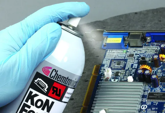
Conformal Coating for SMT Electronics: 50 Key Process Questions Answered
Practical guide to conformal coating in SMT PCB production: methods, defect causes and fixes, curing control, storage, equipment selection, safety, and quality inspection.

Why Must You Pass Through an Air Shower Before Entering an SMT Workshop?
Explains why SMT workshops require air showers: high-velocity airflow and 99.99% filtration remove 0.3 μm particles, reduce ESD, improve placement accuracy, lower solder defects, extend equipment life, and serve as a pressure-buffered barrier.

Why SMT Lines Are Split into Long and Short Lines, and How to Improve SMT Production Efficiency
Learn why SMT lines are divided into long and short configurations and how to boost throughput with planning, line balancing, automation, SPC, and smart material management for high-volume and high-mix environments.

Why Components Must Be Kept Away from PCB Edges: Understanding SMT Rail Keep-Out Zones
Practical DFM guidance on SMT conveyor rail keep-out zones: why 5 mm/4 mm edge clearances exist, risks of violating them, exceptions, and layout tips to protect yield and throughput.

Applying Fishbone Diagram Analysis to SMT Process Defects
Learn how to apply fishbone (Ishikawa) diagrams to SMT process defects. Step-by-step guidance, advantages, and case-focused analysis for open solder, cold solder, and solder bridging to drive evidence-based corrective actions.
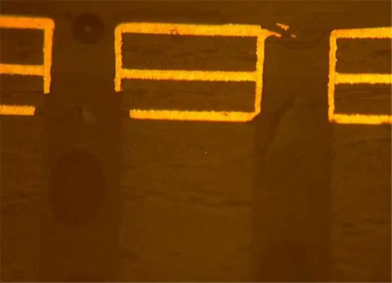
Analysis of PCB Inner-Layer Copper Voids and Hole Breaks: Causes and Corrective Measures
Analyze PCB inner-layer copper voids and hole breaks, covering drilling, desmear, electroless copper, electroplating, dry film, tin plating, and corrective controls.

PCB Panelization Design Optimization and Practical Considerations
Learn PCB panelization methods, including V-scoring, mouse bites, and bridge connections, while optimizing process edges, depanelization, cost, and production efficiency.

Establishing a Precision Stencil Printing Process for Miniaturized Electronics Assembly
Explore precision stencil printing for 01005 and 0.3 mm-pitch assembly, covering area ratio, solder paste transfer efficiency, board support, and process control.


