Destructive dye stain analysis, often called dye-and-pry, is a proven technique for assessing the soldering quality of BGA and other area-array packages. A red penetrant dye is allowed to wick into any microcracks or gaps by capillary action. After drying, the component is forcibly separated so that the fracture surfaces can be inspected. Dyed interfaces indicate open cracks or separations; the extent and location of the dye reveal where the joint failed and whether the failure is due to process defects or post-assembly mechanical stress.
When red dye is observed inside a solder sphere or along an interface, a gap exists at that location—evidence of a crack or incomplete bonding. The fracture surface morphology helps differentiate a latent soldering defect from a crack formed by improper handling or stress during downstream processes.
Dye stain analysis is typically used to investigate BGA soldering issues arising from manufacturing, such as oxidized PCB pads or solder balls, insufficient solder paste coverage on pads, or incorrect reflow/wave solder profiles. If no dye appears on the PCB or BGA pad surfaces but dye can be seen penetrating underneath the pad outline, the root cause is often a PCB or component quality problem such as pad cratering or delamination.
Comparison to Other Analysis Methods
Materials
- Dye: Dykem-80696 (red penetrant dye)
- Cleaning solvent: IPA (isopropyl alcohol)
- Protective gloves
- Pipette or dropper
- Compressed air gun
- Flat-head screwdriver for controlled pry
Characteristics of the Dykem Dye
- Extremely thin, continuous film that resists tearing.
- Strong penetration and fast drying.
- Clearly reveals relative changes at interface surfaces.
- Tolerates scratches, gaps, sharp corners, and surface irregularities.
- Toluene-free.
Recommended Operating Environment
- Perform the process in a dedicated chamber equipped with:
- Exhaust/ventilation system
- Wastewater collection
- Integrated compressed air outlet
- Isolated workspace
- Collect and manage waste dye and solvents after use in accordance with facility controls.
Where to Insert Dye Stain Inspection in a PCBA Flow
- After SMT reflow.
- After DIP wave soldering.
- After ICT on the DIP line.
- After ICT followed by F/T (functional test).
- After packaging of finished or semi-finished assemblies.
Dye Stain Analysis Procedure
Operating Precautions
- Remove any button-cell battery before dyeing. Do not remove other components (e.g., heatsinks) unless they obstruct the dye process; avoid adding mechanical stress to the sample.
- Before dyeing, ensure the cleaning solvent is completely removed with a compressed air gun.
- Dispense dye uniformly along all four sides of the BGA so it can penetrate under the package.
- Allow the oven to reach the set temperature (125 °C) before placing the sample in for drying.
- During component removal, avoid damaging solder balls at the four corners of the BGA.
- Do not touch the fracture surfaces after separation; place the fracture face up for inspection.
- Before analysis, use compressed air to clear debris from the fracture surfaces so loose particles do not confound the results.
Analyzing Dye Stain Results
Analysis Precautions
- Handle separated samples only by the edges; keep fracture faces up.
- Begin with an optical microscope for preliminary inspection, then use a side-view microscope for imaging.
- Use a 2D lens for standard imaging; switch to a rotatable lens if additional angles are needed for determination.
- Capture paired images of each joint: the component-side fracture and the corresponding PCB pad-side fracture.
- Pay particular attention to the four corners, and look for anomalies such as voids and pores in the solder.
SMT Process Verification — BGA Solder Joint Voids
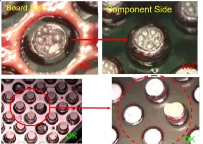
Destructively exposing the BGA cross-section enables direct observation of wetting, voids, and other features indicative of soldering quality.
Acceptance Criteria for BGA Voids
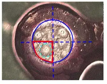
Per IPC-A-610H, the total cross-sectional area of voids shall not exceed 25% of the solder joint's cross-sectional area. The example below illustrates the evaluation method.
PCBA Process Verification — BGA Solder Cracks
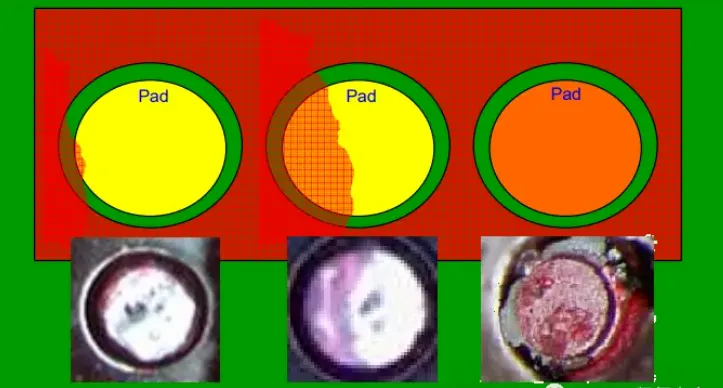
The dye penetration pattern categorizes crack severity:
- Micro crack — Type A
- Partial crack — Type B
- Full crack — Type C
Locations Most Prone to BGA Solder Cracking
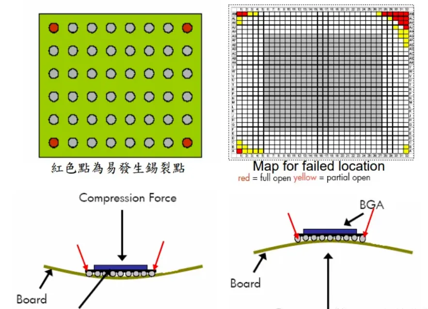
Primary Causes of BGA Solder Cracks
- Poor soldering (e.g., oxidation, insufficient paste, improper profile).
- Improper handling and mechanical shock.
- Depanelization stress.
- Insufficient tooling or support during production steps (e.g., T/U, DIP insertion).
- Poor ICT/ATE fixture design.
- Secondary assemblies such as BIOS socketing or heatsink installation.
- Inadequate packaging materials.
BGA Cross-Section Analysis
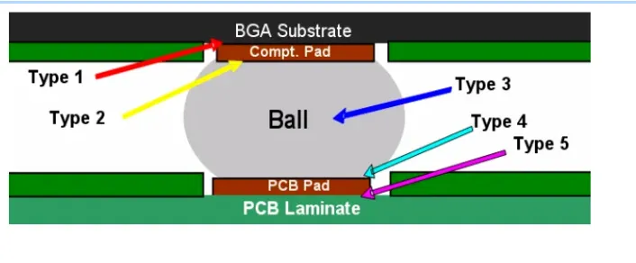
Type 1 & 2: Component Substrate to Component Pad Interface
- Inspect the solder joint morphology for anomalies.
- Dye penetration indicates a crack at the component-side interface.
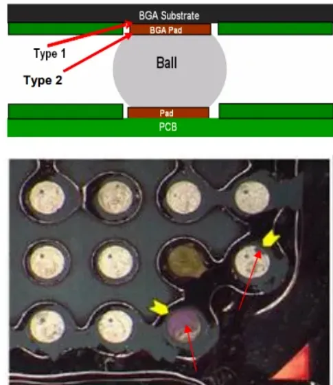
Another example of a crack at the component-side interface:
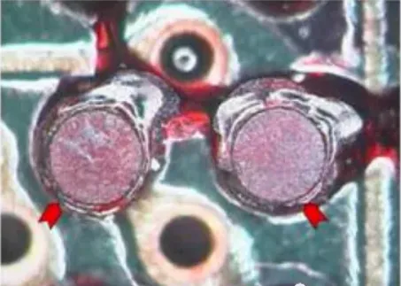
Type 3 & 4: Solder Ball and Solder Ball to PCB Pad Interface
- Check for abnormal voiding in the cross-section.
- Inspect the solder joint appearance.
- Dye penetration indicates a crack at the ball or ball-to-pad interface; such PCB defects often cause test instability or outright failures.
Type 5: PCB Pad to PCB Laminate Interface
- Pad cratering or delamination.
- If no dye penetration is observed during removal, the solder joint is sound.
- If dye penetration is present between the pad and laminate, the assembly was subjected to significant mechanical stress. This defect cannot be repaired by standard rework and should be scrapped.
Alternative Dye Stain Methods
Vacuum Dye Impregnation
- Perform dyeing in a vacuum-capable chamber to encourage thorough penetration.
- Advantage: Maximizes dye infiltration into micro-gaps.
- Disadvantage: Requires cutting the sample from the panel, adding a second stress event that may influence results.
Lever Fixture Removal
- Use a dedicated fixture to apply controlled leverage and remove the component.
- Advantage: Preserves and exposes complete BGA fracture surfaces for inspection.
- Disadvantage: Time-consuming; requires a custom fixture and two-part epoxy and curing adhesive.