A 6 layer pcb mixed signal design works when the analog and digital sections share a continuous ground plane and the noisy edges stay out of the sensitive areas. Fast digital edges and switching supplies inject current into the planes. Low-level analog and reference circuits pick that current up as noise if the return paths are forced to detour or if digital traces run under the analog components. Six layers give enough room for two solid grounds, a power plane, and separate signal routing so the return stays local.
Most mixed-signal problems on these boards start with a ground split that was meant to isolate noise and instead forced every crossing signal to radiate.
Partitioning Analog and Digital Sections
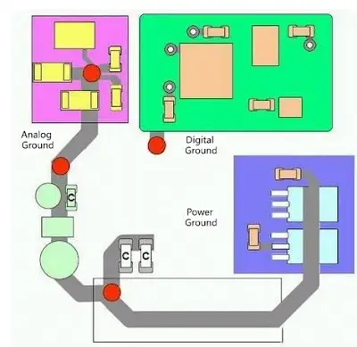
Place the sensitive analog circuitry (op-amps, references, sensor front-ends) in one region and the high-speed digital circuitry (MCU, memory, clocks, interfaces) in another. Put the ADC or DAC at the boundary between the two regions so the conversion interface is short. Route analog signals only inside the analog region on every layer. Route digital signals only inside the digital region. Crossing a digital trace through the analog area couples the edge into the sensitive circuit even if the ground plane is solid. Physical distance helps, but routing discipline does more.
Keep the highest di/dt sources (switching regulators, crystal oscillators, high-speed clocks) as far from the analog inputs as the board outline allows.
Ground Plane Continuity and Return Paths
Use a continuous ground plane under both the analog and digital sections. High-frequency return current concentrates directly under the signal trace on the nearest plane. On a solid ground the digital return stays under the digital traces and the analog return stays under the analog traces. A split forces any crossing net to detour around the gap, increasing loop area and coupling the two domains. Connect the AGND and DGND pins of the converter directly to the same solid plane with short vias. The IC already separates the domains internally; external impedance between the pins couples digital noise back into the analog core.
A split can be used only when no signals cross it and the domains are truly isolated. That case is rare on a mixed-signal board that contains an ADC or DAC.
Isolating High-Speed Digital from Sensitive Analog
Clocks and high-speed data buses carry the fastest edges. Keep them out of the analog region and away from analog traces on adjacent layers. Route them over continuous ground. If a digital net must approach the boundary, keep the parallel run short and place a ground stitch via beside any layer change. Sensitive analog inputs and reference traces should sit over the continuous ground and stay short. Guard traces only help if they are stitched to ground at both ends and at intervals; an unstitched guard can increase coupling. Orthogonal routing on facing signal layers reduces broadside coupling when the stackup forces two signal layers to face each other.
ADC and DAC Local Layout
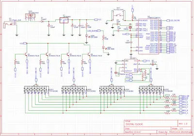
Place the converter at the analog-digital boundary. Keep the analog input and reference traces short and over continuous ground. Place the analog decoupling capacitors right at the AVDD and AGND pins with short, wide connections and multiple vias. Do the same for the digital supply pins. The reference pin often needs its own local capacitor and a quiet trace that does not run near digital edges. Separate the analog and digital supply rails as far as practical, but return both to the same ground plane under the IC. Long traces between AGND and DGND pins or a split under the package itself are common sources of degraded ENOB.
Power Distribution and Decoupling
Use separate analog and digital power rails. Filter or regulate the analog rail so switching noise does not reach the sensitive circuitry. On a 6-layer board one layer can carry the power islands; keep the analog power island over the analog region and the digital power island over the digital region. Pair the power plane closely with a ground plane so the interplane capacitance helps high-frequency decoupling. Place the smallest decoupling capacitors nearest the pins. Stitch the power and ground planes near every high di/dt source and at the board edge. Do not let a digital power island sit under analog signal traces.
6-Layer Stackup Choices for Mixed-Signal
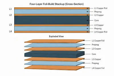
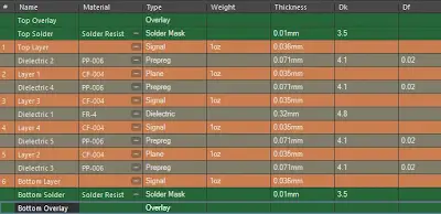
A practical 6-layer PCB arrangement is Signal / Ground / Power / Signal / Ground / Signal. The two ground planes give continuous references on both sides of the inner signal layer and keep return paths short. Another useful option is Signal / Ground / Signal / Ground / Power / Signal when more routing layers are needed next to ground. Put the most sensitive analog nets on the outer layer over the solid ground or on an inner stripline between grounds. Keep high-speed digital on layers that also reference solid ground. Avoid routing critical nets over power-plane splits. The exact order can be adjusted for impedance and thickness, but every signal layer that carries fast or sensitive edges needs a continuous ground reference adjacent to it.
Common Mixed-Signal Mistakes on 6-Layer Boards
The most frequent problem is a ground split under a signal that must cross domains. The return detours, the loop grows, and the noise appears at the analog input. Running a digital clock or high-speed bus through the analog region produces the same result even with a solid plane. Placing the converter deep inside one region instead of at the boundary lengthens the interface and forces more crossings. Missing stitch vias at layer changes near the boundary or under the converter package leaves the return free to spread. Power islands that extend under the wrong section or decoupling capacitors placed too far from the pins let switching noise reach the reference. On a 6 layer pcb mixed signal design the continuous ground and the routing discipline set the noise floor. The layer count only helps if those two rules are followed.