The stack note that still shows up is "FR-4, Dk 4.5." No frequency. No Df. Widths sized from that number. Length matching done in CAD inches as if every layer flies at the same speed. Then the first multi-gigabit interface fails timing or loss and the laminate gets blamed as if it changed after Gerbers.
FR4 PCB Dk Df is not a pair of catalog adjectives. Dk sets how fast the edge moves and how wide the trace has to be for a target Z0. Df sets how much of that edge you still have at the far end. Use the 1 MHz datasheet pair on a 5 GHz net and both numbers are already wrong before etch starts.
Dk Is Delay and Impedance, Not a Material Nickname
Dk is εr. Velocity is c / √Dk_eff. Z0 moves as 1/√Dk. That is the electrical job of the number. Tg and CTI are a different conversation.
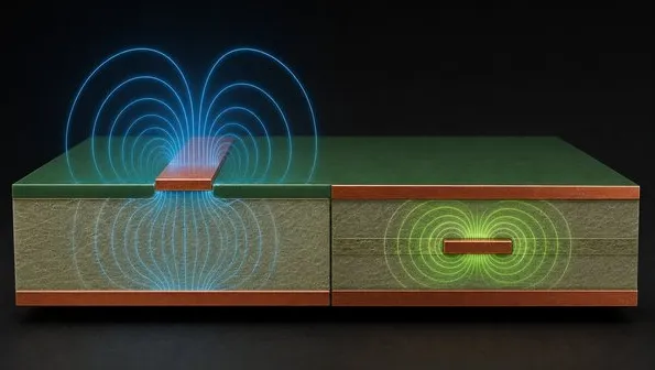
Bulk Dk on commodity FR4 is typically 4.2–4.8 at 1 MHz. The trace does not see that. Microstrip has air above the copper; Dk_eff lands closer to 3.2–3.8. Stripline is buried, so Dk_eff is closer to the laminate. Same core, two speeds. Matching an outer pair to an inner pair in raw millimeters is a delay error wearing a length-match report.
Resin content and glass style move Dk more than the marketing name. 1080-heavy prepreg is resin-rich and lower Dk. 7628 is glass-heavy and higher. Swap 2116 for 1080 to hit finished thickness and you change height and εr together. Width stays. Z0 and flight time do not.
Df Is the Loss You Do Not Get Back at the Receiver
Df is tan δ. Dielectric attenuation rises with frequency and with Df. On short FR4 runs, conductor loss still owns most of the budget. Df takes the rest, and it keeps taking as the bit rate climbs.
Standard FR4 is commonly quoted around Df 0.020 at 1 MHz. That quote is almost useless on a 5–8 Gb/s edge. At gigahertz, mid-grade FR4 is often still 0.015–0.020. Mid-loss sits nearer 0.008–0.012. Low-loss is a different resin, not a tighter etch note on the same 150 °C book.
You cannot compensate Df with width the way you compensate Z0. Wider copper helps conductor loss. The dielectric is still the dielectric. Equalization buys some of it back. It cannot invent a laminate you did not stack.
The 1 MHz Datasheet Number Is Not Your Edge Rate
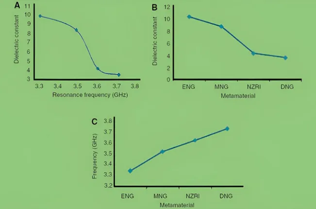
Dk on FR4 falls as frequency rises, then flattens. The drop from 1 MHz to 1–2 GHz is the one that surprises people who sized 50 Ω from the datasheet cover. A few tenths of Dk is a few ohms of Z0 and a few percent of delay. Inside a ±10% impedance window. Not inside a tight length-match budget.
Df does not stay put either. Treat 1 MHz tan δ as a family flag, not a loss model. If the vendor publishes Dk/Df at 2 GHz and 10 GHz, use those. IPC-4101 slash sheets name the class. They do not give you one εr for every net.
Moisture raises both. A board that sat open after bake does not have the same FR4 dielectric constant signal integrity numbers as a dry coupon. Matters more on a long lossy run than on a 20 mm USB pair. Still a real shift.
Glass weave is local Dk, not average Dk
A 0.10 mm pair can sit over a resin channel next to a glass bundle. Local εr swings. Delay and Z0 swing with it. The fat impedance coupon averages that out. Length matching in the router does not see it. Tight timing on a narrow outer pair over coarse 7628 is the usual miss. Spread-glass or a finer style is the material fix. Routing at an angle is the layout fix. Neither appears if you only wrote "Dk 4.5 typ."
What Those Numbers Do to Flight Time and Insertion Loss
Outer FR4 microstrip is roughly 140–160 ps/inch with a realistic Dk_eff. Buried stripline on the same laminate is closer to 160–180 ps/inch. A match report that treated every layer as 150 ps/inch is why source-synchronous budgets still fail. Use the stack you bought, not the constraint-manager default.
A 10% error in assumed Dk is about 5% in delay. On a 150 mm run that is 20–30 ps. Harmless on GPIO. Enough to eat DDR or SerDes margin that vias and packages already spent.
Loss is the other half. Short nets at a few hundred megahertz are still conductor-dominated. Long inner pairs at several gigahertz are not. Standard FR4 near Df 0.02 ships USB 3.x and PCIe Gen3 on short fanouts every day. Stretch it across a 10–12 inch 10G path and the eye is a stackup problem you should have named before placement.
Rough copper stacks with high Df. A simulator that used smooth foil and 1 MHz Df reads optimistic. The TDR coupon proves Z0. It does not prove insertion loss.
Where Commodity FR4 Stops Being the High-Speed Answer
Standard FR4 is the right call for short controlled-impedance digital. USB, HDMI, GbE, LVDS, MIPI, PCIe Gen3 on a few inches. The interface budget assumed that family. A fancier resin does not fix a split plane or a stub.
Wrong call when the loss budget is already spent: long 10G / 25G, PCIe Gen4/5 across a backplane-length board, analog that cares about loss flatness, RF that needs published Dk at the band. Then specify mid-loss or stop calling it FR4. Routing tighter does not lower tan δ.
Do not swap constructions silently. Prototype on characterized mid-loss, production on the cheapest 150 °C book with "Dk 4.5" in the notes. Same outline. Different delay. Different dB. The fab holds thickness. They do not hold an electrical model you never named.
Hybrid stacks only work if the drawing names the prepreg and the frequency the Dk/Df pair was measured at. "FR-4 equivalent" is not a dielectric model.
What Belongs on the Stack Note Instead of "Dk 4.5"
Name the laminate family and the frequency for Dk and Df. 1 MHz is fine only if the fast nets are short and you are not treating it as a 10 GHz model. Prefer vendor data at 2 GHz or 10 GHz for anything you will simulate above a gigahertz.
Lock glass style on the pair layers. Weave risk means spread glass or route off-axis — not a tighter impedance tolerance. Separate microstrip and stripline delay. Match in time, or at least use the right ps/inch per layer.
Use Df to decide whether standard FR4 belongs in the conversation. Short multi-Gb/s: usually yes. Long or next-gen SerDes: price mid-loss before placement freezes. A loss sim with real Df and roughness is cheaper than a respin after the first eye.
The factory will press the book you allowed. They will etch the width that hits the Z0 coupon. They will not correct a 1 MHz εr you used at 8 Gb/s, and they will not reduce tan δ because the title block said "high speed."
FR4 PCB Dk Df only help signal integrity when the numbers match the frequency, the construction, and the length. Dk is how fast and how wide. Df is how much arrives. Write both at the frequency the edge actually occupies. Everything else is a datasheet cover used as a field-solver input.