The note that causes the most argument is not the 50 Ω target. It is the ±5% next to it. Copied from an RF module drawing onto a four-layer USB board. Or the opposite: a blank tolerance field, so CAM treats the class as "etch to artwork" and the coupon is optional.
FR4 PCB impedance tolerance is not how close your field solver sat to the schematic number. It is the window the factory is allowed to miss on a measured coupon after etch, press, and mask. Write a window the stack can actually hold, or you buy scrap and a conversation about whose calculator was right.
Tolerance Means the Coupon, Not the CAD Width
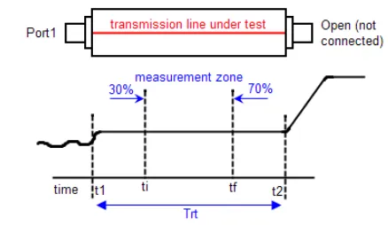
Target Z0 is a geometry. Tolerance is a process result. TDR on a coupon built in the same panel as the board. Same copper weight, same prepreg lot, same mask. Not a screenshot from Saturn or Polar taken before the stack was locked.
50 Ω ±10% is 45–55 Ω. 90 Ω differential ±10% is 81–99 Ω. 100 Ω ±10% is 90–110 Ω. That is the commercial window most FR4 houses already run. The coupon fails or it does not. Your 0.127 mm trace in CAD is not evidence either way.
IPC-6012 treats controlled impedance as a specified requirement, not a default class attribute. If the drawing does not list target, type (SE or diff), layer, reference, finished copper, mask on or off, and tolerance, there is no requirement. "Impedance control required" with no table ships as standard etch.
±10% Is the House Process. ±5% Is a Quote Change.
Default PCB impedance tolerance on commodity FR4 is ±10%. USB 2.0 / 3.x, HDMI, DisplayPort, 1000BASE-T, LVDS, most PCIe Gen3 fanouts live in that window every day. The interface budgets assumed a few ohms of mismatch. They did not assume a laboratory stack.
±8% is the next step that still ships without a special laminate conversation, if the geometry is stripline or a well-controlled outer microstrip and CAM is allowed to compensate width. ±5% on outer masked microstrip is where yield and price both move. Mask thickness, etch trapezoid, and prepreg flow each take a bite. There is not much left for the laminate Dk you did not pay for.
±5% on 50 Ω is 47.5–52.5 Ω. A 2 Ω soldermask shift plus a 3 Ω etch miss already spends the budget. Inner stripline is easier — no mask, dielectric on both sides, less sensitivity to one-sided etch. That is why the same fab will hold ±7% buried and struggle at ±5% on L1.
Do not put one tolerance on every class. 50 Ω RF drop to an SMA is not the same ask as a 100 Ω HDMI pair that runs 40 mm. Tight on the RF. Commercial on the HDMI. A single ±5% line in the title block is how GPIO nets grow coupons and cost. Tighter window also means characterized prepreg, CAM compensation, sometimes 0.5 oz start copper, sometimes mid-loss instead of the cheapest 150 °C Tg core. None of that appears if you only typed a tighter percentage.
Dk and Prepreg Height Spend the Budget Before Etch Starts
Z0 on microstrip moves with dielectric height and with 1/√Dk. A 10% swing in h is not a 10% swing in Z0 — typical outer geometries move something like 4–8%, depending on width-to-height. Thin prepreg is worse. 0.075–0.10 mm glass is already near the press-out limit. Lot-to-lot resin content is a real number, not a footnote.
The datasheet Dk is usually 1 MHz. Your edge is not. Standard FR4 Dk falls as frequency rises. Using 4.5 at 1 MHz to size a 5 GHz pair puts you a few ohms off before the first panel. Mid-loss and "impedance-controlled FR4" grades publish Dk at 2 GHz or 10 GHz. If you specified ±5% and then allowed "FR-4, Tg 150, Dk 4.5 typ," you specified two things that do not coexist.
Glass weave is local Dk. A 0.10 mm pair sitting over a resin channel next to a 7628 bundle sees a different εr than the fat coupon. Length matching will not catch that. Tight tolerance on a narrow outer pair without a weave note is optimism.
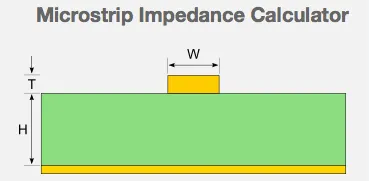
Etch, Mask, and Finished Copper Are the Rest of the Miss
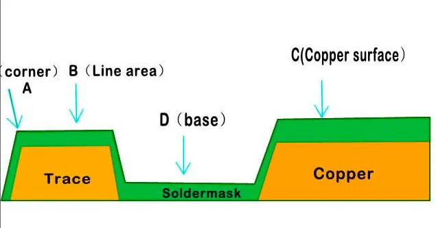
Artwork width is not finished width. The wall is a trapezoid. 1 oz finish is thicker than 1 oz foil. CAM offsets the film so the coupon lands in the window. "Do not touch my widths" plus a tight FR4 PCB impedance tolerance is two notes that cancel. Pick one.
Soldermask on microstrip lowers Z0 a few ohms. Calculators that assume bare copper read high. The coupon includes mask. If your stack note is silent on mask, the first article will come back 3–5 Ω low and someone will blame Dk.
Differential gap is etch-sensitive. A 0.10 mm gap on 1 oz is where the process lives at the edge. Tight ±5% on 90 Ω outer pairs with a minimum gap is how coupons fail even when single-ended 50 Ω on the same layer passes. Widen the pair or bury it before you tighten the percentage.
Press-out changes h after you froze the width. Prototype on 1080, production on 2116 because purchasing found a cheaper book — same finished board thickness, different dielectric over L2. Widths stay. Z0 does not. Lock the construction, not just the overall mils.
How to Write a Tolerance the Fab Can Hold
Start from the interface, not from a round number that looks careful. If the spec and the length say ±10% keeps the eye open, write ±10%. Save ±8% or ±5% for the nets that actually lose margin — RF launches, long multi-Gb/s runs, analog front ends that sit on a defined Z0.
Ask the house what they already hold on that construction. A four-layer 1.6 mm FR4 with 0.10–0.18 mm L1–L2 prepreg and 1 oz finish will quote ±10% without a meeting. The same shop will tell you ±5% outer needs 0.5 oz, characterized prepreg, and CAM compensation. That answer is the design constraint. It is not a negotiation after Gerbers.
Put the table on the fabrication drawing. One row per class. Layer and reference named. Masked microstrip called out. Finished copper, not foil. Tolerance next to the target. Allow CAM to compensate — if the pair is already at minimum width and gap, you left no room to correct etch. That is a layout problem wearing a percentage.
A passing coupon does not bless a pair that crossed a split or sat on a resin pocket. Tolerance is stack plus etch. Return path and weave are still yours.
What to Put on the Drawing Before the Stack Freezes
List only the classes that need a coupon. Assign ±10% unless the interface or the length says otherwise. If you need ±5%, say which layer, accept 0.5 oz or stripline, and lock a characterized FR4 — not a generic Dk 4.5 line.
Do not tighten tolerance to paper over a two-layer 1.6 mm stack that cannot make 50 Ω at a usable width. Do not leave tolerance blank and assume the factory will guess ±10%. The coupon is the contract. The percentage is how wide you made that contract.
Specify FR4 PCB impedance tolerance the way you specify drill tolerance: as a window the process already owns, on the geometries you actually routed. ±10% is the normal answer. ±5% is a stack and a process, not a more serious font in the notes.
```