The drawing says 90 Ω. The pair is the right width. Then it crosses a gap between two ground islands, or rides a power pour that stops at a connector cutout. The coupon still passes. The interface does not. Impedance was never only the trace. It was the trace plus the copper it returns on.
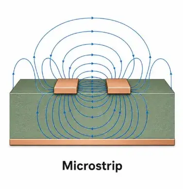
A FR4 PCB reference plane is that copper. Ground, usually. Sometimes a quiet power plane if the stack forces it. Continuous under the route, close enough that the field stays in the dielectric you paid for. Split it, and the return takes a detour. EMI and a broken edge show up before the fab ever sees a yield problem.
The Plane Is Half the Transmission Line
Return current at a fast edge does not wander the shortest DC path. It stays under the trace, in the region of lowest loop inductance. That is the adjacent plane. Cut the plane and the current still has to close. It goes around the slot. Loop area grows. The "50 Ω" geometry you calculated no longer exists for that segment.
On FR4, the useful reference is the next copper layer, not the far side of a 1.6 mm core. Four-layer L1 over L2 ground is the normal stack because the field is short. Same width over L4 is a different Z0 and a much larger loop. Calling L4 the reference because the net name is GND does not change the physics.
Power can be a reference if it is solid, stitched, and bypassed at the layer change. A 3.3 V pour full of thermal reliefs and voltage islands is not that plane. Mixed-signal boards like to keep analog ground "clean" by splitting it under a USB pair. The pair does not care about your analog story. It cares that its return just hit a slot.
Why the Reference Gets Cut During Layout
Placement wins first. A connector row, a DC-DC, a crystal can, and someone needs a pour to sneak through. The plane layer is the easiest place to steal copper. Or analog and digital grounds get split at a ferrite with the split drawn as a moat across the whole board. Fast nets are routed later. They inherit the moat.
Via antipads punch holes. A BGA escape on a dense FR4 four-layer can Swiss-cheese L2 until the "solid ground" under the SerDes pair is a ladder of voids. The plane looks continuous in the 2D viewer at 50 %. Zoom to the pair pitch and it is not.
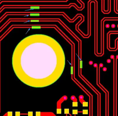
Layer changes without a nearby return via do the same job. The signal leaves L1. The return stays on L2 until it finds a ground via. That hop is a slot in Z. One ground via at the pin is not a fence. Thermal isolation around a regulator, a mechanical keepout, a copper-free strip — all legal in CAM. All a slot if a high-speed net crosses them.
What a Split Does to Return Current
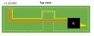
The return follows the trace until the gap. Then it runs the edge of the pour to the nearest bridge — a capacitor, a stitch via, a connector shell, the board outline if you left it that bad. That path is common to every other net using the same plane edge. Crosstalk that was geometry-limited becomes a shared inductance problem.
Differential pairs are not immune. The odd mode still wants a local return in the plane. A split under both members is a common-mode antenna. Tight coupling helps only while both traces see the same reference. The instant one member hangs over the gap and the other does not, the pair is two single-ended lines with a slot in the middle.
EMI is the usual field failure. The extra loop radiates. A USB or HDMI cable becomes the rest of the antenna. ESD and surge follow the same slot if it reaches a connector. Signal integrity is the quieter failure: a shelf in the edge, a mode conversion that eats the eye after three inches of otherwise correct geometry.
Continuous Plane Rules That Survive FR4 Stackups
Keep one solid reference under every net you treated as a transmission line. Ground is first choice. If the stack puts a power plane next to the signal layer, that power net has to be one voltage, unbroken under the route, and tied to ground with vias and capacitors at both ends of any layer change.
Do not split analog and digital ground under a fast interface. Split, if you must, where no fast edge lives — and then stitch the two grounds at one point that is not in the return path of USB, HDMI, PCIe, DDR, or the clock. A ferrite across a moat that a pair still crosses is a bead in series with the return. That is worse than no split.
Via fences at layer changes: ground vias next to the signal vias, not three millimeters away "because the channel was full." For a differential pair, two grounds flanking the pair is the minimum that actually closes the loop. Antipads on the reference layer should not merge into a slot along the escape. If L2 is lace under the BGA, move the pair or add a plane layer.
Crossing from one plane region to another needs a stitch cap at the crossing, not a PDN cap on the other side of the IC. On a 200 ps edge, "nearby" is a few millimeters.
How High-Speed Layout Should Treat the Plane, Not Just the Trace
Place the connectors and the PHY so the pair can stay on one layer over one plane for as long as the budget allows. Every layer hop is a reference change you have to buy back with vias. Fan out, then run. Do not weave L1–L3–L1 to dodge a crystal can if L2 under that detour is already cut.
Route the critical nets before you fragment the plane with pours and voids. Plane leftovers after routing are how splits appear. If a power neck has to cross the high-speed channel, change the stack or the placement. Do not notch L2 to feed a regulator and then declare the pair "referenced to GND."
Two-layer FR4 is the stack that cannot keep a close reference. The far-side ground is too far for a 0.15 mm trace to be 50 Ω, and every through-hole and connector cutout is a slot in the only plane you have. If the interface needs a defined high speed PCB reference plane, four layers with thin prepreg to L2 is the layout decision. Width tweaks on 1.6 mm two-layer are not.
Keep fast copper several line widths inside a solid pour. The internal edge — split, antipad row, thermal island — is the electrical slot. Length-match after the reference is frozen. Matching across a gap equalizes two bad returns. The TDR coupon sits on intact stack. Your pair does not.
CAM will etch the width. They will not pour copper you deleted, and they will not add stitch vias you did not place. A plane split is a layout decision that survives every impedance note on the drawing.
Design the FR4 PCB reference plane first: one solid return under the fast nets, close in the stack, stitched at every layer change, never crossed by a moat. Then set width and gap. The high-speed problem on FR4 is usually not the laminate. It is the return path the layout opened after the stack was already chosen.