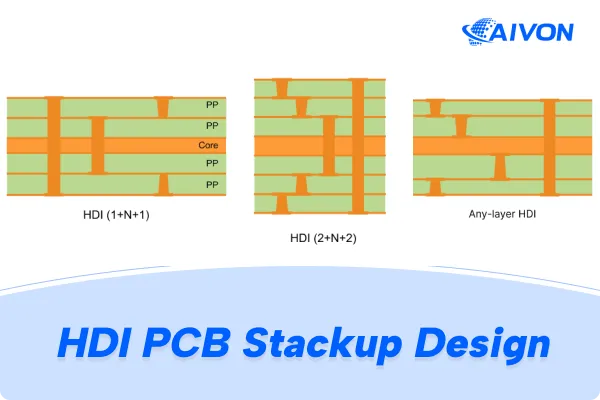
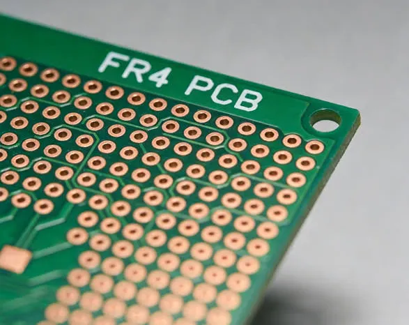
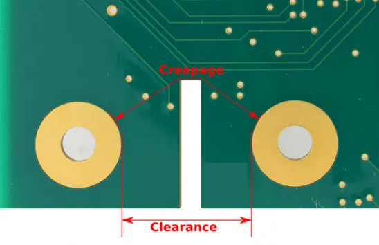
Copper thickness and minimum trace width are not independent variables in HDI. They are linked through the physics of etching. Thicker copper produces greater lateral undercut during the etch process. That undercut directly reduces the final conductor width and forces the designer to start with a larger artwork feature or accept a wider finished trace. Ignoring the relationship produces either open circuits, uncontrolled impedance, or a board that the fab cannot yield.
The connection between HDI copper thickness trace width is one of the most frequent sources of design-rule violations and late-stage engineering queries. It is also one of the easiest to get right if the etch behavior is treated as a fixed constraint rather than an afterthought.
Why Thicker Copper Raises the Minimum Trace Width
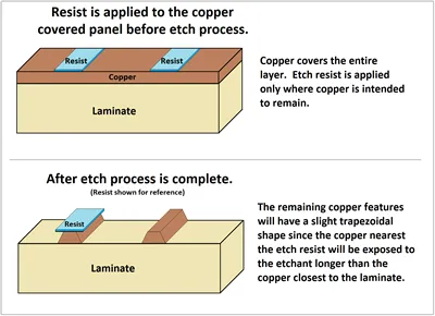
Etching removes copper from the top surface and from the sidewalls simultaneously. The deeper the copper, the longer the etch must run to clear the field, and the more time the sidewalls are exposed to the etchant. The result is a trapezoidal cross-section whose base is narrower than the original photoresist opening.
On thin copper (9–12 µm or ¼–⅜ oz) the undercut is small and fine features remain predictable. On standard 1 oz (35 µm) copper the undercut is already significant. On 2 oz (70 µm) or heavier copper the lateral etch can easily consume 20–40 µm per side. A trace that was drawn at 75 µm in artwork may finish at 40 µm or less—or disappear entirely if the process is not tightly controlled.
This is why HDI processes that advertise 50 µm traces almost always assume thin copper on the outer layers. Specifying those same traces on heavy copper moves the design outside the process window.
Etch Undercut and the Need for Artwork Compensation
To obtain a finished trace of a target width, the artwork must be drawn wider by approximately twice the expected undercut per side. The compensation factor is process-dependent and increases with copper thickness. A fab may require 15–20 µm total compensation for 1 oz copper and 30–50 µm or more for 2 oz copper.
If the designer draws the finished width and the fab applies its standard compensation, the final copper is narrower than intended. Clearances shrink, impedance rises, and current-carrying capacity drops. If the designer over-compensates, the finished traces become wider than the impedance model assumed and adjacent clearances may be violated.
The correct sequence is to obtain the fab's compensation table for the specific copper weight and then draw the artwork accordingly. Treating compensation as a global number independent of copper thickness is a common error.
Impedance and Current-Carrying Trade-Offs
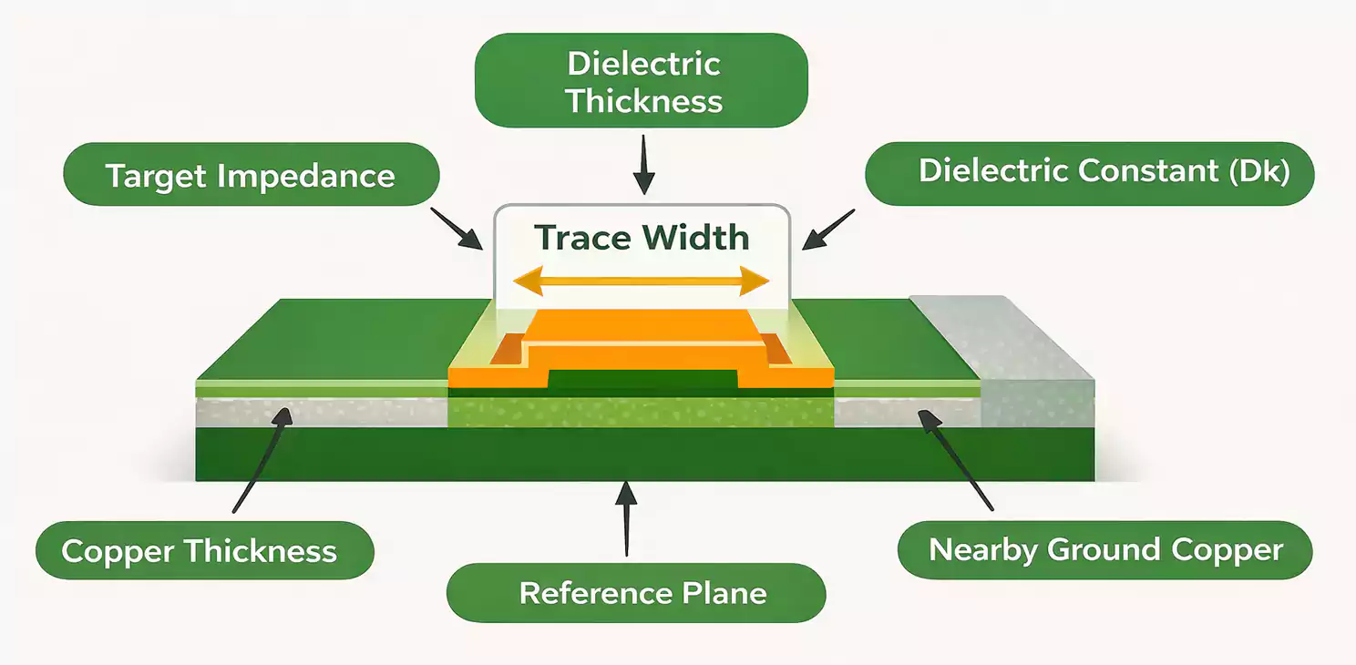
Thicker copper lowers the characteristic impedance of a trace of given width because the conductor cross-section increases and the current distribution changes. To hold the same impedance, the designer must either widen the spacing to adjacent copper or reduce the trace width. Reducing the width on thick copper is exactly the direction the etch process resists.
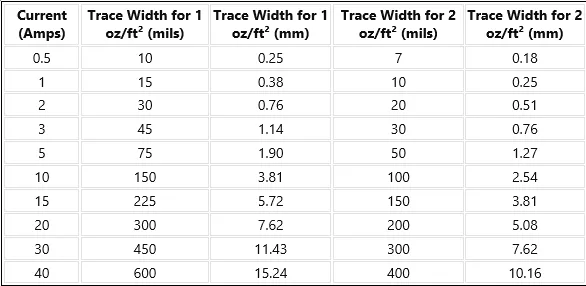
Current capacity moves in the opposite direction. Heavier copper allows higher current for the same width or a narrower width for the same current. When a net must carry significant current and also meet a tight impedance target, the two requirements pull against each other. The usual resolution is to use thicker copper only on power layers or on short high-current segments, while signal layers stay on thinner copper that supports fine HDI features.
Attempting to satisfy both high current and fine-pitch HDI routing on the same heavy-copper layer forces compromises in either impedance control or manufacturability.
Common Pairing Errors Seen in Design Reviews
The most frequent mistake is pairing 50–60 µm traces with 2 oz or heavier copper on outer layers. The combination looks attractive for current capacity and density, but the etch process cannot hold the geometry. Yield drops and the finished width becomes unpredictable.
Another common error is calculating impedance for a finished width while drawing the artwork at that same width, then sending the files to a fab that applies its own compensation. The resulting board has higher impedance and reduced current capacity than the model predicted.
Designers also mix copper weights across layers without adjusting the design rules for each weight. A stack-up that uses 1 oz on signal layers and 2 oz on power layers needs two different minimum trace/space rules. Applying a single fine-line rule to the entire board produces violations on the heavy-copper layers.
Confirming Capability Before the Design Rules Are Frozen
The only reliable way to set HDI copper thickness trace width rules is to obtain the fab's capability table for the exact copper weights planned in the stack-up. That table should list minimum finished trace and space, recommended artwork compensation, and the process tolerance on final width.
Ask for data on the specific dielectric and plating process that will be used, not generic brochure numbers. Laser-drilled HDI layers with thin dielectric often run thinner copper than the core layers; the rules must reflect that difference.
Once the numbers are confirmed, lock the design rules by copper weight. Signal layers that need fine features stay on the copper weight that supports them. Power layers that need current capacity use the heavier copper and accept the wider minimum features that come with it.
Practical Relationship That Survives Production
Thinner copper enables finer traces and tighter impedance control at the cost of lower current capacity. Thicker copper provides current capacity and mechanical robustness at the cost of larger minimum features and more difficult etch control. The two cannot be optimized simultaneously on the same layer without compromise.
The relationship is fixed by the etch process. Design rules that respect the undercut behavior of the chosen copper weight produce boards that etch cleanly and meet both impedance and current targets. Rules that ignore the relationship produce late-stage changes, yield loss, or both. Confirming the fab's actual capability for each copper thickness before the stack-up is finalized remains the simplest way to keep HDI copper thickness and trace width in productive alignment.