From a fabrication standpoint, the choice between sequential build-up (SBU) HDI and traditional multilayer PCBs is driven by routing density and via structure more than by marketing claims. Traditional multilayer boards remain the default for moderate complexity designs because the process is mature, stable, and lower cost. Sequential build-up becomes necessary when blind and buried microvias, finer lines, and higher interconnect density are required. Most shops push designers toward traditional multilayer first and only move to SBU when the design cannot be routed or the form factor forces it.
The trade-off is clear: sequential build-up delivers higher density and better electrical performance in compact packages, but it increases process steps, registration risk, and unit cost. Understanding where that cost and complexity start to pay off is the practical decision most engineers need.
Where Sequential Build-Up and Traditional Multilayer Separate
| Factor | Traditional Multilayer | Sequential Build-Up (HDI) |
|---|---|---|
| Typical layer count | 4–16 layers (common up to 20+) | Often 6–14 with 1–3 build-up layers per side |
| Via structure | Through-hole vias, some buried | Microvias, blind/buried, stacked or staggered |
| Routing density | Moderate; limited by drill size and pad size | High; fine lines and microvias free up routing channels |
| Manufacturing complexity | Lower; single or few lamination cycles | Higher; multiple sequential laminations and laser drills |
| Registration risk | Moderate | Higher with each additional build-up cycle |
| Cost (same layer count) | Baseline | 30–100 %+ higher depending on build-up count |
| Lead time | Shorter and more predictable | Longer; more process steps and inspection points |
| Typical applications | Industrial controls, power, standard computing | Smartphones, wearables, high-speed modules, dense BGA |
Decision Matrix for Design and Production Priorities
| If your priority is… | Better Choice | Why |
|---|---|---|
| Lowest cost and stable yield | Traditional Multilayer | Fewer process steps, mature equipment, higher first-pass yield |
| Highest routing density or fine-pitch BGA | Sequential Build-Up | Microvias and thinner cores free routing space |
| Fast prototype and predictable lead time | Traditional Multilayer | Shorter process flow and wider supplier base |
| Thin overall board thickness with many layers | Sequential Build-Up | Build-up layers allow thinner dielectric and better control |
| High-volume consumer electronics | Sequential Build-Up | Density enables smaller form factors that justify cost |
| Industrial, power, or moderate-density designs | Traditional Multilayer | Adequate performance at significantly lower fabrication risk |
Layer Count and Stack-Up Reality
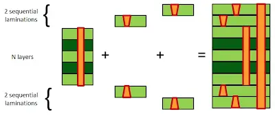
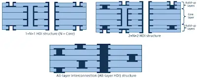
Traditional multilayer boards are laminated in one or a few cycles. All layers are typically bonded together after inner-layer imaging and etching. Sequential build-up starts with a core (often 2–6 layers) and then adds dielectric and copper layers one side at a time, drilling and plating microvias after each build-up cycle. This allows thinner dielectrics and more precise control of impedance, but each additional sequential cycle multiplies registration and yield risk.
In production, a 1+N+1 or 2+N+2 structure is common. Going beyond three build-up layers per side becomes expensive and yield-sensitive. Traditional multilayer can reach higher total layer counts more economically when density is not the limiting factor.
Routing Density and Via Technology Differences
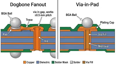
The core advantage of sequential build-up is the ability to use laser-drilled microvias (typically 75–150 µm) that land on capture pads without consuming large through-hole real estate. This frees routing channels and allows finer escape from dense BGAs. Traditional multilayer relies primarily on mechanical through-hole vias whose diameter and pad size limit how tightly components can be placed and how many signals can escape a high-pin-count package.
From a CAM perspective, designs that require via-in-pad or stacked microvias almost always force sequential build-up. Designs that can be routed with through-hole and standard buried vias stay on the traditional process for better cost and yield.
Manufacturing Complexity and Process Risk
Traditional multilayer processing is well understood: inner-layer fabrication, oxide treatment, lamination, drilling, plating, and outer-layer imaging. Sequential build-up adds laser drilling, sequential lamination, and multiple plating cycles. Each build-up layer introduces new opportunities for registration error, resin voids, and via plating defects. Yield typically drops with every additional sequential cycle.
In the factory, SBU boards require tighter process control, more advanced laser and registration equipment, and more intermediate inspection. Traditional multilayer runs on a wider range of equipment with higher first-pass yields. This difference becomes noticeable in both prototype and volume production.
Cost Differences That Matter at Scale
Material cost is only part of the story. Sequential build-up multiplies process steps: extra lamination cycles, laser drilling, and plating. Even when the finished layer count looks similar, an HDI board with two build-up layers per side can cost 50–100 % more than a traditional multilayer of the same total layers. The premium is justified only when the density gain reduces overall system size or enables a design that cannot be routed otherwise.
At low volumes the cost gap is especially large because setup and engineering time for SBU is higher. At high volumes the gap narrows but rarely disappears. Most manufacturers recommend staying with traditional multilayer unless the routing or form-factor requirements clearly demand HDI.
Application Scenarios and Design Constraints
Traditional multilayer boards dominate industrial controls, power supplies, automotive body electronics, and many computing boards where component density is moderate and cost sensitivity is high. Sequential build-up is preferred for smartphones, tablets, wearables, high-speed networking modules, and any design that must escape fine-pitch BGAs in a small footprint.
Signal integrity and power integrity can also favor HDI because shorter via stubs and tighter layer spacing reduce parasitics. However, these benefits only matter when the design actually uses the higher density. Many boards that are converted to HDI "just in case" end up carrying unnecessary cost without performance gain.
How PCB Factories Evaluate Sequential Build-Up vs Traditional Multilayer
During DFM and CAM review the first questions are via structure and minimum feature size. If the design can be routed with mechanical through-holes and standard line/space, we recommend traditional multilayer. When laser microvias, via-in-pad, or multiple sequential layers appear, the design is flagged for HDI capability review. We check registration budgets, dielectric thickness capability, and whether the chosen build-up structure (1+N+1, 2+N+2, etc.) matches the fabricator's process window.
Process risk is higher with sequential build-up because each lamination cycle compounds dimensional change and registration error. Yield models are more conservative, and first-article inspection is more rigorous. Panel utilization can also be affected by the need for tighter process control and more test coupons. Most shops will suggest design changes that reduce the number of sequential cycles or convert stacked microvias to staggered where possible to improve yield and lower cost.
In production planning, traditional multilayer offers more capacity flexibility and shorter lead times. Sequential build-up occupies specialized laser and sequential lamination lines that are often capacity-constrained. This difference shows up clearly in both prototype and volume scheduling.
Which Option Should You Choose?
Choose traditional multilayer if you:
- Have moderate routing density and can use through-hole or standard buried vias
- Need the lowest possible board cost and highest production yield
- Require fast prototype turns and predictable lead times
- Are working with industrial, power, or non-miniaturized designs
- Want a wider choice of fabricators and more stable process capability
Choose sequential build-up HDI if you:
- Must escape fine-pitch BGAs or achieve very high interconnect density
- Need thinner overall board thickness with multiple layers
- Require microvias, via-in-pad, or stacked via structures for electrical or space reasons
- Are designing compact consumer, mobile, or high-speed modules where size justifies cost
- Can accept higher fabrication cost and longer lead time for the density benefit
In many cases the optimal solution is a hybrid approach: keep the majority of the board on traditional multilayer technology and introduce limited sequential build-up only in the densest regions. This balances density needs against cost and yield. Always start the design with the simplest via and layer strategy that meets the electrical and mechanical requirements, then escalate to sequential build-up only when necessary.
Frequently Asked Questions
Q1: Is sequential build-up always more expensive than traditional multilayer for the same layer count?
A1: Yes in nearly all cases. The extra lamination cycles, laser drilling, and tighter process controls add cost even when total copper layers look similar. The premium typically ranges from 30 % to over 100 % depending on the number of build-up layers.
Q2: When does routing density force a move to sequential build-up?
A2: When fine-pitch BGAs (typically 0.5 mm or below) cannot be escaped with through-hole vias, or when the required line/space and via density exceed what mechanical drilling and standard multilayer processes can support. At that point microvias become necessary.
Q3: How many sequential build-up layers are practical in production?
A3: Most fabricators handle 1+N+1 and 2+N+2 reliably. Three or more build-up layers per side are possible but yield and cost degrade quickly. Designs should minimize sequential cycles wherever possible.
Q4: Does sequential build-up always improve signal integrity?
A4: It can, because microvias have shorter stubs and tighter layer spacing is achievable. However, the benefit only appears when the design actually uses the higher density and controlled stack-up. Simply converting a traditional board to HDI without changing the routing rarely produces meaningful SI improvement.
Q5: Is traditional multilayer still suitable for high-speed designs?
A5: Yes for many applications. With proper stack-up design, controlled impedance, and careful via management, traditional multilayer boards support multi-gigabit signals. HDI becomes preferable mainly when density or form-factor constraints force it.
Q6: What is the biggest manufacturing risk with sequential build-up?
A6: Registration and yield loss across multiple lamination cycles. Each sequential step introduces dimensional change and alignment error. Poor process control leads to open or shorted microvias and higher scrap rates compared with traditional multilayer.