Two Layers Stay Cheaper Until Routing or EMI Forces a Plane Pair
The 2 layer vs 4 layer FR4 PCB decision is a construction call, not a material swap. Both boards use the same glass-epoxy family. What changes is whether the shop images and laminates inner copper, and whether the finished book has a dedicated reference plane under the signals. From a fabrication standpoint, a 2-layer FR4 board is the better manufacturing choice when the netlist finishes on two surfaces, currents are modest, and EMC can be closed with layout discipline and a few copper pours. A 4-layer FR4 board is the better choice once you need a continuous ground (and usually a power) plane, controlled impedance, or enough routing channels that a 2-layer design starts jumping with via forests.
We normally recommend staying on 2-layer FR4 for power adapters, LED drivers, simple analog, through-hole industrial boards, and cost-driven consumer work that never sees a BGA or a fast edge. We recommend moving to 4-layer when CAM review shows crowded jumpers, broken return paths, a named 50 Ω / 90 Ω / 100 Ω spec, or an EMI failure that copper pours will not fix. Jumping to 4-layer "to be safe" on a board that only needs two copper faces is how unit cost rises without changing the product.

What Separates a 2-Layer FR4 Board from a 4-Layer Book on the Floor
| Factor | 2-layer FR4 PCB | 4-layer FR4 PCB |
|---|---|---|
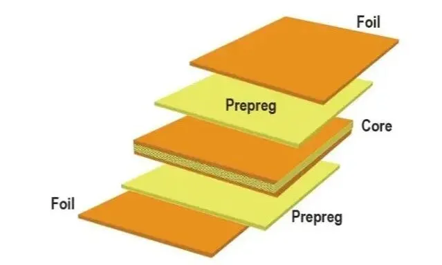
| Layer structure | Double-sided CCL; no inner image, no multilayer press | Core + prepreg + foil; inner etch, oxide, one lamination |
| Typical stack-up | L1 signal/mix — core — L2 signal/mix | L1 signal / L2 GND / L3 PWR / L4 signal (most common) |
| Routing space | Two faces only; pours compete with traces | Two outer routing layers plus optional inner routing; planes free the outers |
| Signal integrity / EMI | Broken returns; pours are not a plane | Continuous reference; impedance and loop area become controllable |
| Controlled impedance | Possible but unstable; reference is a pour, not a plane | Production default for 50 Ω microstrip and 90/100 Ω pairs |
| Manufacturing complexity | Drill, plate, outer image; widest process window | Adds inner image, inner AOI, brown oxide, press, registration |
| Finished-board cost | Baseline for a given outline and copper weight | Typically ~1.4–2.2× the 2-layer price at the same size and qty |
| Yield / process risk | Highest; fewest process steps | Still high on standard FR4; inner opens/shorts and misreg appear |
| Prototype lead time | Same-day to 48 h on most standard lines | Usually 3–5 working days; press and inner AOI add a queue |
| Typical applications | Adapters, LED, simple MCU, through-hole industrial | MCU + comms, mixed-signal, USB/Ethernet, coarse BGA, EMC-sensitive |
A drawing that only says "FR4, 1.6 mm" is not a layer decision. CAM needs layer count, which layers are planes, copper weight per layer, and whether impedance is required. Without that, a 2 layer vs 4 layer PCB quote is just a guess at process steps.
Which Layer Count Wins When the Priority Changes
| If your priority is... | Better choice | Why factories lean that way |
|---|---|---|
| Lowest board cost and shortest proto queue | 2-layer FR4 | No inner process, no press; scrap is cheap |
| Highest first-pass fab yield | 2-layer FR4 | Fewer operations; inner etch and lamination defects do not exist |
| Mass production of a simple power or analog board | 2-layer FR4 | The 4-layer premium never pays back if two faces close the netlist |
| Controlled impedance or fast digital edges | 4-layer FR4 | A pour is not a reference plane; stack-up geometry only exists with inner copper |
| EMI / return-path integrity | 4-layer FR4 | Continuous GND under signals shrinks loop area in a way 2-layer pours cannot |
| Dense SMD, coarse BGA, or mixed analog/digital | 4-layer FR4 | Planes free outer channels and keep analog returns off digital dumps |
| Board size reduction without shrinking parts | 4-layer FR4 | Moving power and ground inside recovers routing real estate on L1/L4 |
| Widest supplier list | Either, but 2-layer is slightly wider | Almost every rigid shop runs both; 2-layer still starts faster |
How the Layer Book Is Actually Built
On a 2-layer FR4 PCB the starting material is a double-sided copper-clad core. The shop drills, metallizes the holes, images and etches both faces, then finishes. There is no inner-layer artwork and no multilayer press. Thickness is the core thickness plus copper and solder mask. That is why 2-layer jobs move through CAM and the drill room with almost no stack-up debate.
A 4-layer FR4 PCB starts as an inner core that is imaged and etched first. After inner AOI and oxide, prepreg and copper foil are laid up on both sides and pressed. From drill onward the traveler looks like a 2-layer job, but the book now has four copper faces and a registration budget between inner and outer. The common production stack is signal–GND–PWR–signal on 1.6 mm or 1.2 mm finished thickness. Signal–GND–GND–signal is used when the design is more EMI-driven than power-distribution-driven. Mixed inner routing on L2 or L3 is possible, but every trace cut into a plane is a slot in the reference — CAM flags that during DFM because it undoes part of why you paid for four layers.
The structural difference that matters in production is not "more copper." It is the presence of continuous inner sheets that can be used as planes. Without those sheets, a 2 layer vs 4 layer FR4 PCB comparison collapses to two routed faces versus four routed faces, which is the wrong model for most 4-layer work.
Where Routing Space Actually Runs Out on Two Layers
Routing space is the first place the 2 layer vs 4 layer PCB comparison stops being theoretical. On two layers every net, every pour, every thermal relief, and every connector pin fights for the same two faces. A ground pour that is cut into islands by traces is not a plane; it is leftover copper. Designers then add vias to jump signals from top to bottom, and those vias punch holes in whatever pour was left. During CAM review we see this as via density climbing in the MCU neighborhood, long detours around connectors, and 5/5 mil traces used not because the shop needs them but because there is nowhere else to go.
Four layers do not magically add two extra routing canvases on a typical FR4 stack. L2 and L3 are usually planes. What you buy is the ability to pull power and ground off the outer faces so L1 and L4 can be used as routing layers instead of mixed power-signal patchwork. That is the real capacity gain. If the design still cannot escape after that, the next step is not "more vias on 2-layer." It is either a tighter line/space on 4-layer or a move to 6-layer. Trying to keep a dense digital board on 2-layer by dropping to 3/3 mil and filling the board with jumpers raises fab risk and still leaves the return-path problem untouched.
From a fabrication standpoint we also watch panel utilization. A 2-layer board that grows 15–20% in outline just to finish routing can erase the layer-count saving. Quote both constructions on the same outline first. If the 2-layer version only works after the board gets larger, the 4-layer unit cost often wins once assembly and enclosure size are included.
Why Signal Integrity Changes More Than Layer Count Suggests
Signal integrity is where 2-layer FR4 and 4-layer FR4 stop being interchangeable even if both boards route. On two layers the return current has to find a pour, a stitch via, or a detour around a slot. Fast edges (USB, Ethernet PHY, MCU clocks, switching edges on a DC-DC) radiate from that loop. Impedance is whatever local copper happens to sit under the trace, so a "50 Ω" note on a 2-layer drawing is rarely a number the shop can hold from coupon to coupon.
On a 4-layer FR4 PCB the outer traces sit over a continuous ground or power plane at a known dielectric thickness. That geometry is what makes microstrip impedance a production item: we adjust line width against the pressed dielectric, not against a patchy pour. Differential pairs pick up a consistent odd-mode reference. Loop area drops because the return sits a few tenths of a millimeter below the trace instead of centimeters away on the opposite face. That is the performance comparison that actually shows up in EMC chambers and in eye diagrams — not "four layers are faster."
The trade-off here is honesty about edge rate. A slow analog front end, a relay board, or a line-frequency power stage does not need that plane. Putting those products on 4-layer FR4 improves nothing the customer will measure. Putting a 100 MHz-class digital section on 2-layer and then buying ferrite beads and a shield can to pass EMC is how the "cheaper" construction becomes the expensive one after the first compliance spin.

Where the Manufacturing Cost Starts to Diverge
Cost is the question every RFQ asks first in a 2 layer vs 4 layer FR4 PCB comparison, and the answer is not "twice the layers, twice the price." A 4-layer board adds inner imaging, inner AOI, oxide, lamination, and more copper and prepreg. It does not double drill hits, surface finish, routing, or electrical test in proportion. In production we typically see finished-board prices land around 1.4–2.2× a same-size 2-layer FR4 board at medium volume. Prototypes sit at the high end because the inner and press steps have a minimum lot charge. Large panels of a simple 4-layer consumer board sit at the low end.
What moves the multiple is not layer count alone. Copper weight (2 oz inner or outer), impedance coupons, tight registration, high-Tg FR4 instead of standard Tg, and extra surface-finish area all add more dollars on 4-layer than they do on 2-layer because they ride on a more expensive traveler. Conversely, a 2-layer board that needs 2 oz copper, heavy milling, and a large outline can price closer to a light 4-layer than buyers expect.
Lead time follows the same split. Most shops can start a 2-layer FR4 job the same day from stocked cores. A 4-layer job waits on inner etch and a press opening. That is usually two to three extra working days on a standard prototype line, not weeks — unless the stack calls a non-stock core thickness or a locked laminate brand. For mass production the difference shrinks because both constructions run in scheduled lots; the unit-cost gap remains.
How the Shop Reads 2-Layer Versus 4-Layer During DFM
During CAM review the first filter is whether the netlist can close without violating the shop's standard line/space and via pad. On 2-layer FR4 we look at via count per square centimeter, pour fragmentation, and whether power traces are being asked to carry current that belongs on a plane or a poured pour with thermal vias. If the designer has already dropped to the shop's minimum trace to finish the board, we flag the job as "2-layer at the edge." That board will yield, but the next ECO that adds a connector usually will not.
On 4-layer FR4 the review shifts to stack-up and planes. We check that L2/L3 are actually planes rather than leftover routing layers with random cuts, that via antipads do not chew the reference under critical pairs, and that the dielectric after press supports the impedance table on the drawing. Registration between inner and outer is a real process item; it is also a mature one. Yield on a standard 4-layer FR4 panel is still high. What drops yield is not "four layers" — it is inner shorts from dirty etch, misregistration on a tight BGA fan-out, or a press that was asked for an unusual dielectric height without a process coupon.
Process risk and inspection follow the traveler. 2-layer work is outer AOI plus electrical test. 4-layer work adds inner AOI before the book is closed; after that, inner defects are only visible as opens/shorts at E-test or as impedance coupon misses. Most manufacturers therefore recommend 4-layer only when the electrical or density need is real, and they recommend keeping the 4-layer stack on a shop-standard 1.6 mm or 1.2 mm book with 1 oz copper unless the drawing gives a reason not to. Non-standard cores and odd finished thicknesses are how a simple layer upgrade turns into a materials delay.
Panel utilization is similar for both if the outline is the same. The factory does not prefer 2-layer because it "fits more on a panel." It prefers 2-layer because the process is shorter and the scrap cost of a bad panel is lower. Once the design needs planes, that preference flips: running a marginal 2-layer that fails EMC or assembly is worse for everyone than a clean 4-layer on a standard stack.
When Staying on Two Layers Stops Being the Right Call
The upgrade question is the one that should close the 2 layer vs 4 layer FR4 PCB comparison. We normally recommend moving to 4-layer when any of the following shows up in review or in the lab — not when a checklist says "modern boards have four layers."
Upgrade when routing only finishes by using the shop's minimum line/space across large areas, when via fields sit under an MCU or a coarse BGA just to jump nets, or when a ground pour is so slotted that return current has no continuous path. Upgrade when the drawing names controlled impedance, USB, Ethernet, LVDS, or a clock edge that already failed EMC on a 2-layer spin. Upgrade when analog and switching nets share a face and the only isolation tool left is physical distance you no longer have. Upgrade when shrinking the outline matters more than the layer premium — moving planes inside is often cheaper than a larger 2-layer board plus a larger housing.
Do not upgrade when the product is a linear power stage, a simple sensor, an LED string, or a through-hole controller that already passes on two faces. Do not upgrade to solve a thermal problem that needs copper weight or a metal core rather than extra layers. Do not upgrade as a substitute for a bad component footprint. And do not skip from 2-layer to 6-layer because 4-layer "might not be enough." Close the netlist on four layers with planes first; 6-layer is the next conversation after that stack is honestly full.
Which Construction to Release
Choose a 2-layer FR4 PCB if you:
- Can finish every net on two faces at the shop's standard line/space without a via forest
- Have no controlled-impedance callout and no high-speed interface that already failed EMC
- Are building adapters, LED, simple analog, or through-hole industrial boards
- Need the lowest unit cost and the shortest prototype queue
- Want the highest first-pass fab yield on a high-volume panel
Choose a 4-layer FR4 PCB if you:
- Need a continuous ground (and usually power) plane under the signals
- Have USB, Ethernet, LVDS, or another spec that needs a real impedance stack
- Are mixing analog and digital on a tight outline, or escaping a coarse BGA / dense SMD field
- Failed EMC on a 2-layer pour and the next lever is loop area, not another bead
- Can keep L2/L3 as planes on a shop-standard 1.2 mm or 1.6 mm FR4 book
There is no single winner in the 2 layer vs 4 layer FR4 PCB comparison. Two layers are the manufacturing default. Four layers are the manufacturing tool for routing space, return path, and impedance that two faces cannot close. The right release is the cheaper construction that still routes, still yields, and still passes EMC — not the one with more copper on the traveler.
Questions That Show Up on 2-Layer vs 4-Layer Quotes
Q1: Is a 4-layer FR4 PCB always about twice the price of a 2-layer board?
A1: No. For the same outline, copper weight, and quantity, most shops land around 1.4–2.2×. Inner process and extra laminate drive the delta; drill, finish, and test do not scale with layer count. Prototypes sit higher because of lot charges.
Q2: Can a 2-layer FR4 PCB meet a 50 Ω impedance spec?
A2: On paper, if a solid pour sits under the trace at a known height. In production the pour is usually slotted, so the coupon and the board disagree. If impedance is a real requirement, 4-layer with a dedicated reference plane is the construction we quote to.
Q3: Does moving from 2-layer to 4-layer always improve EMI?
A3: Only if L2/L3 stay continuous planes and critical traces sit over them. A 4-layer book with inner routing slots cut through the ground plane can radiate like a messy 2-layer board. The plane is the feature, not the layer count.
Q4: When is 4-layer not enough and we should go to 6-layer?
A4: When the two outer layers cannot finish routing even with planes on L2/L3, when you need a clean split between analog and digital references, or when a second signal pair must sit between planes for stripline. Do not skip 4-layer as a habit.
Q5: Is 4-layer FR4 harder for the factory to yield than 2-layer?
A5: Slightly. Inner etch, oxide, press, and registration add defect opportunities. On a standard 1.6 mm FR4 stack with ordinary line/space, first-pass yield is still high. Yield drops when the stack is non-standard or the inner artwork treats planes as leftover routing.
Q6: What must be on the drawing before we can quote 2 layer vs 4 layer PCB accurately?
A6: Layer count, finished thickness, copper weight per layer, which layers are planes, impedance targets if any, minimum line/space and via size, and outline. "FR4, 1.6 mm" does not tell the shop whether to image inners or book a press.