HDI Is a Build Method on FR4, Not a Replacement Laminate
The FR4 vs HDI PCB comparison is a construction decision, not a material swap. Almost every production HDI board is still an FR4 (or mid/high-Tg FR4) stack. What changes is how the layers connect: a standard FR4 multilayer uses mechanically drilled plated through-holes that punch the full thickness; an HDI PCB adds laser microvias, buried vias, and sequential lamination so signals can drop one or two layers at a time instead of consuming a drill channel through the whole book.
From a fabrication standpoint, standard FR4 is the better manufacturing choice when BGA pitch is 0.8 mm or coarser, routing can finish on 4–8 through-via layers, and the shop does not need via-in-pad. HDI is the better choice when 0.5 mm and finer packages, via-in-pad, or a thin finished thickness force you off the mechanical-drill line. We normally recommend staying on through-via FR4 until CAM can show that the escape or the layer count actually fails — jumping to 1+N+1 because "HDI sounds denser" is how quotes inflate without changing the product.
Read "FR4 PCB vs HDI" as through-via FR4 versus HDI-on-FR4. Changing the dielectric (Rogers, polyimide, metal core) is a second comparison on top of the via structure.

What Separates Through-Via FR4 from HDI Before CAM Releases the Job
| Factor | Standard FR4 multilayer | HDI PCB (typically FR4-based) |
|---|---|---|
| What it actually is | Glass-epoxy laminate + mechanical PTH | Same family of laminate + laser microvias and sequential build-up |
| Via structure | Through-hole, optional buried; drill ≥0.2 mm typical | Microvia 75–150 µm, buried via, via-in-pad; stacked or staggered |
| Routing density | 3/3 mil possible; 4/4–5/5 is the production window | 3/3 common; 2/2 on advanced lines; via-in-pad frees channels |
| BGA escape | Comfortable at 0.8 mm; 0.5 mm needs extra layers or dog-bone | Preferred at 0.5 mm and required for most 0.4 / 0.35 mm packages |
| Manufacturing complexity | One press cycle, one drill program on a standard line | Laser, fill/cap, extra press cycles, tighter registration |
| Finished-board cost | Baseline for the same outline and copper area | 1+N+1 often ~1.3–1.8×; 2+N+2 and any-layer climb faster |
| Layer-count trade | Density is bought with more layers and more PTH real estate | Can drop 2–4 layers versus a through-via book of equal escape |
| Yield / process risk | High on ordinary 4–8 layer work | Lower; fill voids, stacked-via cracks, and sequential misreg show up in X-ray |
| Lead time / supplier base | Almost any rigid shop; cores on the shelf | Needs a laser + via-fill line; fewer qualified vendors |
| Typical applications | Industrial control, power, 0.8 mm+ compute, through-hole connectors | Phones, wearables, camera modules, SiP, thin 0.4–0.8 mm boards |
A drawing that only says "HDI, FR4, 8L" is not a spec. CAM needs the build type (1+N+1, 2+N+2, any-layer), which layers carry microvias, stacked versus staggered, whether microvias are copper-filled and capped, and the finished aspect ratio. Without that, the FR4 vs HDI PCB quote is a guess.
Which Construction Wins When the Priority Changes
| If your priority is... | Better choice | Why factories lean that way |
|---|---|---|
| Lowest board cost and widest supplier list | Standard FR4 | No laser, no fill, one lamination; scrap is cheap |
| 0.4 mm or finer BGA / CSP escape | HDI | Mechanical PTH pads eat the channel under the package |
| Via-in-pad under a fine-pitch part | HDI | Filled microvias are the production method; tented PTH is not |
| Fast prototype on a standard line | Standard FR4 | Most shops can start the same day; HDI CAM and laser queue add days |
| Cut an 12–16 layer through-via book down | HDI (often 1+N+1 or 2+N+2) | Microvia escape can retire two to four layers and still net lower cost |
| Mass production of a 4–8 layer industrial board | Standard FR4 | HDI premium never pays back if pitch and thickness do not require it |
| Finished thickness under ~0.6 mm with inner routing | HDI | Through-drill aspect ratio and stub length become the limit first |
| Highest first-pass yield | Standard FR4 | Fewer process steps; stacked-via and fill defects are HDI-specific |
FR4 and HDI Share the Same Laminate Family — The Via Structure Does Not
This is the point most RFQs get wrong in the FR4 vs HDI PCB comparison. FR4 names the dielectric. HDI names the interconnect architecture. You can build HDI on standard-Tg FR4, high-Tg FR4, halogen-free FR4, or a hybrid core. You cannot "order HDI instead of FR4" the way you order Rogers instead of FR4.
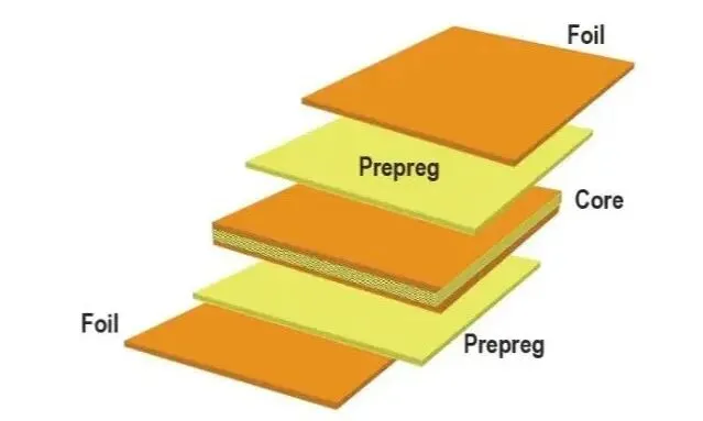
What the factory changes is the build sequence. A standard FR4 multilayer is cores plus prepreg, one press, mechanical drill, PTH plate, outer image. An HDI board adds a laser dielectric (RCC, laser-drillable prepreg, or a thin core), laser ablation, desmear, copper plate, usually a fill-and-cap, then another press for the next build-up pair. 1+N+1 is one extra cycle per side. 2+N+2 is two. Any-layer is a different shop capability.
During CAM review we first ask whether the stack is even HDI. A board with 0.25 mm through-holes, 5/5 mil, and no via-in-pad is a standard FR4 job even if the title block says HDI. A 0.4 mm BGA with via-in-pad on a "normal 8-layer FR4" drawing is an HDI job whether the buyer used the word or not.
Microvias Change Escape, Aspect Ratio, and What the Plating Line Must Do
The microvia is the feature that makes HDI worth the extra steps. A typical production microvia is 75–100 µm at the top, laser-ablated through 50–80 µm of dielectric, with aspect ratio held near 0.8:1 to 1:1. That geometry plates. Push the dielectric thicker or the hole smaller and the barrel becomes a void risk. Standard FR4 through-holes live in a different window: 0.2–0.3 mm drill in 1.6 mm stock is routine; the same drill in 0.4 mm stock wastes pad area the HDI stack would have given back.
Via-in-pad is where the two constructions stop being interchangeable. A PTH in an SMT pad has to be filled and capped or it steals solder, and the pad still has to clear drill plus annular ring. On HDI, copper-filled laser vias sit inside the BGA pad, get planarized, and drop the dog-bone from the escape. That is the difference buyers are paying for — not a different resin.
Stacked versus staggered is the next factory fork. Staggered microvias are kinder to plating. Stacked vias save X-Y area and need a qualified fill, a flat cap, and a press that leaves copper — not a dimple — for the next laser. We normally recommend stagger until the pitch forces a stack.

Routing Density Is Bought With Vias First, Trace Width Second
Line and space get the attention in any FR4 PCB vs HDI discussion. In production, via real estate usually runs out first. A through-via with a 0.5 mm pad blocks a channel on every layer it pierces. That is why an 8-layer through-via board still cannot escape a 0.5 mm BGA without jumping to 10 or 12 layers. HDI keeps that via on L1–L2. Layers 3–N stay available for planes and long routes.
Trace geometry still matters. A capable FR4 line holds 4/4 mil with yield to spare and 3/3 mil on 18 µm copper. HDI shops that already run laser registration typically hold 3/3 as default and 2/2 on a qualified outer process. Pushing 2/2 on a through-via-only shop is usually a worse idea than adding a 1+N+1 pair.
Signal integrity follows the via, not the name. A short microvia has less stub than a 1.6 mm PTH used only on L1–L2. That helps at a few gigahertz. It does not turn FR4 into a low-Dk laminate. If Df is the constraint, change the resin; do not assume HDI beats a back-drilled FR4 stack on loss.
Where the Manufacturing Cost Starts to Diverge — and Where HDI Can Cost Less
Board price stalls most FR4 vs HDI PCB quotes. A 1+N+1 coupon of the same outline and copper area as an 8-layer through-via FR4 board typically lands at 1.3–1.8× after laser time, via fill, extra press, and poorer panel utilization. 2+N+2 moves past 2×. Those multipliers assume the layer count stays the same. That assumption is often wrong.
The comparison that matters in CAM is a 12-layer through-via FR4 that barely escapes versus an 8-layer 1+N+1 that escapes cleanly. The HDI board can land at or below the 12-layer price because you dropped prepreg, inner images, and a long drill program — and finished thickness, which is what the mechanical team wanted. We see that swap on modules more often than on industrial controllers.
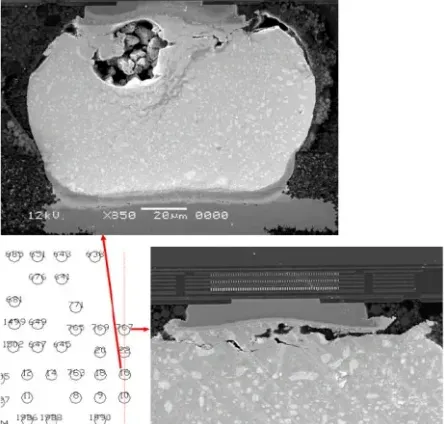
Hidden cost sits in yield. Every extra sequential cycle is another chance for misregistration or a fill void that only X-ray catches. HDI scrap is expensive because the panel already carries laser and plate time. A standard FR4 6-layer panel that fails AOI is cheap to write off. That is why factories push back on HDI when the pitch does not require it.
How the Factory Reads an FR4 vs HDI Package in DFM
On the DFM desk the first filter is capability. Does this plant have laser, via-fill plate, and a sequential-press recipe for that dielectric thickness? If not, the job is a through-via FR4 redesign or it leaves the building. Shops that only drill PTH should not "try HDI" on a production lot.
When the line can build both, CAM checks build type (1+N+1 / 2+N+2 / any-layer) with microvia layers named; microvia diameter versus dielectric thickness; stacked or staggered plus fill-and-cap for via-in-pad; and whether a through-via redesign still closes at the stated pitch.
Panel utilization is the quiet yield killer. HDI coupons want more microsection real estate, so the working panel carries fewer parts. Inspection is heavier: AOI on every build-up layer and X-ray on stacked vias. Lead time stretches with each press cycle. A standard FR4 8-layer prototype can leave in a few days; the same outline as 2+N+2 waits on two extra laminations and two laser programs.
What we typically recommend: stay on through-via FR4 when pitch is 0.8 mm and layer count is already comfortable. Move to 1+N+1 when a 0.5 mm package or via-in-pad appears, or when four extra through-via layers would cost more than one laser pair. Reserve 2+N+2 and any-layer for 0.4 mm and below, or for thickness a PTH aspect ratio cannot support.
Which Option You Should Release — By Pitch, Thickness, and Volume
Choose standard through-via FR4 if you:
- Are escaping 0.8 mm or coarser packages without via-in-pad
- Can finish the netlist on 4–8 layers at 4/4 or 3/3 mil
- Need the widest supplier base and the shortest prototype queue
- Are building industrial, power, or connector-heavy boards where PTH is a feature
- Want the highest first-pass yield on a volume panel
Choose HDI (usually still on FR4) if you:
- Have 0.5 mm parts that force extra layers on a through-via book, or 0.4 / 0.35 mm packages
- Need copper-filled via-in-pad under a BGA, LGA, or CSP
- Can drop two to four layers versus the through-via alternative and recover the process premium
- Need finished thickness in the 0.4–0.8 mm range with inner routing
- Have named the build type, microvia layers, fill spec, and stagger/stack on the drawing
Stay on FR4 material and only change the via structure if you:
- Do not have an RF loss or high-temperature reason to leave glass-epoxy
- Can meet Tg and CAF with mid- or high-Tg FR4 already on the HDI line
- Would otherwise mix a laminate change and an HDI change in one spin — that hides which variable failed
There is no single winner in the FR4 vs HDI PCB comparison. Standard through-via FR4 is the manufacturing default. HDI is the manufacturing tool for pitch, via-in-pad, and thickness that the default cannot close. The right release is the cheapest construction that still escapes and still yields — not the one with more process steps on the traveler.
Questions That Show Up on FR4 vs HDI Quotes
Q1: Is an HDI PCB made from a different material than FR4?
A1: Usually no. HDI describes microvias and sequential lamination. Most production HDI boards are FR4 or high-Tg FR4 with a laser-drillable outer dielectric. Call the laminate and the build type as two separate line items.
Q2: When does FR4 PCB vs HDI stop being optional?
A2: When the package pitch or via-in-pad requirement makes a through-hole pad too large to escape, or when finished thickness makes the PTH aspect ratio unreliable. 0.4 mm-class parts and sub-0.8 mm boards are the usual trip points.
Q3: Why can an HDI board cost less than a standard FR4 board?
A3: Only when HDI retires layers. A 1+N+1 8-layer that replaces a struggling 12-layer through-via design can win on laminate, drill time, and finished thickness. Same layer count, same outline — HDI costs more.
Q4: Is 1+N+1 enough, or do we need any-layer?
A4: 1+N+1 covers a large share of 0.5 mm work and many via-in-pad layouts. Any-layer is for stacked escape on very fine pitch or very thin stacks. Specifying any-layer by default raises cost and cuts the supplier list without helping the netlist.
Q5: Do microvias always improve signal integrity versus FR4 through-holes?
A5: They shorten the unused via stub, which helps. They do not change Dk or Df of the resin. For loss-limited channels, pick the laminate first, then pick through-via, back-drill, or microvia as the stub tool.
Q6: What must be on the drawing before a factory will quote FR4 vs HDI?
A6: Build type (1+N+1, 2+N+2, any-layer), microvia layers and diameters, stacked or staggered, copper-fill and cap requirement, finished thickness, BGA pitch, and minimum line/space. "HDI FR4, 8L" is not a stack-up.