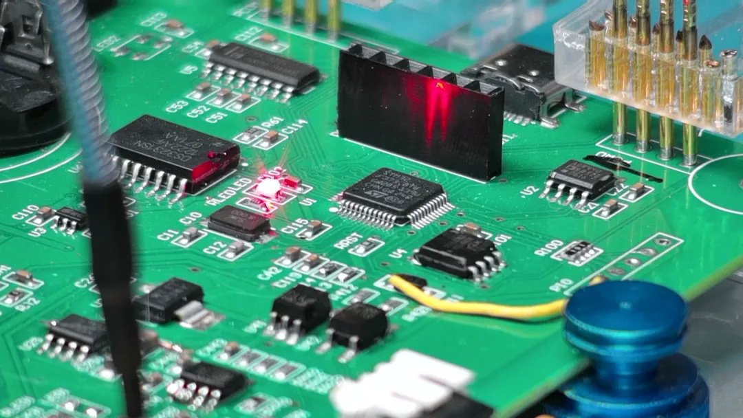
Have you ever wondered why a smartphone wakes up the instant you press its power button, or how a computer CPU can process information billions of times per second? Behind these capabilities is an inconspicuous but nearly ubiquitous device: the MOSFET, or metal-oxide-semiconductor field-effect transistor. It acts like a miniature intelligent water gate in the electronic world, controlling the flow of current and serving as a fundamental building block of modern electronics.
The MOSFET is a basic unit of integrated circuits. In digital circuits, MOSFETs implement the switching behavior required to represent logic 0 and logic 1. A MOSFET has three primary terminals: the source, gate, and drain. Its simplified structure is shown below.

During MOSFET fabrication, the layout and interconnection of the source, gate, and drain are critical. The precision of these structures directly affects device performance and reliability. In logic gates, MOSFETs work together with other transistors to implement a wide range of Boolean functions.

Arithmetic units are built from carefully combined logic gates. These gates act as key nodes in a circuit, using precise switching operations to create the complex functions required for computation. Ultimately, such logic gates are integrated into chips that may be only about the size of a fingernail.
Why Do We Need Electronic Switches?
Consider a conventional light switch. When it is pressed, a metal contact closes the circuit and the lamp turns on. When it is released, the contact separates, opening the circuit and turning the lamp off. This mechanical approach is simple and reliable, but it is far too slow, large, and power-hungry for high-speed processors and mobile devices.
Modern chips require a switch with several essential characteristics:
- Extremely high speed: It must be able to switch billions of times per second.
- Very small size: It must be sufficiently small for billions of devices to fit on a chip only a few square centimeters in area.
- Low power consumption: The switching control itself should consume very little power.
- High control sensitivity: A small electrical signal must be able to control current through the main conduction path.
The MOSFET provides these characteristics and is therefore one of the most important electronic switches ever developed. The electronic switches inside a chip are the foundation for computation, storage, signal routing, power management, and control.
What Do MOSFETs Do Inside a Chip?
Building Logic Gates
The most fundamental function of MOSFETs is to build logic gates, which provide the decision-making functions of digital circuits. In a simple inverter, the switching state of a MOSFET converts an input logic level into the opposite output level. When the input is high, the transistor configuration can cause the output to be pulled low. When the input is low, the output can be pulled high through the complementary transistor network.
The basic functional units of a digital chip are logic gates such as AND, OR, and NOT gates. These gates determine how input signals represented by 0 and 1 are combined to produce an output. A simple NOT gate can be implemented with MOSFETs, while more complex gates are created by connecting multiple MOSFETs in carefully designed networks.
Large numbers of logic gates form the arithmetic logic unit, control unit, registers, and other core blocks of a CPU. The arithmetic logic unit performs operations such as addition and subtraction, the control unit coordinates circuit operation, and registers temporarily hold data. Without transistor switching, a processor could not perform computation or make decisions.
Storing Information
MOSFETs are also essential to memory circuits. In SRAM, a storage cell commonly uses four or six MOSFETs to form two cross-coupled inverters. The two stable states of this circuit—one output high and the other low, or the reverse—represent logic 0 and logic 1. MOSFETs control the establishment, retention, and reading of these states.
A DRAM cell uses a MOSFET switch together with a capacitor. The transistor controls access to the capacitor:
- Writing a 1: The switch turns on and the capacitor is charged to a high level.
- Writing a 0: The switch turns on and the capacitor is discharged to a low level.
- Reading: The switch connects the capacitor to the sensing circuitry so that its charge state can be detected.
The MOSFET determines when charge may enter or leave the capacitor and when the stored state may be read. Without this access switch, the charge would not be properly controlled and the memory cell could not reliably store information.
Routing Signals
Modern chips contain enormous numbers of interconnections. Data must move rapidly and accurately among logic units, registers, and memory cells. MOSFET switches act as controlled junctions in this internal routing network.
- Multiplexers and demultiplexers: MOSFET switching networks select which input signal is allowed through or determine which path receives an output signal.
- Bus switches: They control whether different circuit blocks can access a shared data bus.
- Clock distribution: Switching structures help control when clock signals reach different regions of a chip.
These switches ensure that the correct data travels along the correct path at the correct time. Without controlled routing, signals from different blocks could conflict and the internal information flow would become unreliable.
Managing Power Consumption
MOSFETs are also central to power management inside integrated circuits. Clock gating disables the clock signal to a block that is not currently needed. When the clock stops toggling, the block’s dynamic power consumption can be greatly reduced.
Power gating uses dedicated MOSFET power switches to disconnect the supply rails of a circuit block that will remain inactive for a longer period. Disconnecting its VDD or GND supply can substantially reduce leakage-related or standby power consumption.
Power management can therefore be implemented at a fine granularity, allowing selected blocks to remain active while others enter a low-power state. Without these switching techniques, every circuit block would continue operating continuously, resulting in excessive power consumption and heat generation.
Dynamic power is consumed when a MOSFET changes state and charges or discharges the interconnect and load capacitances connected to it. Static power may also exist even when a transistor is not switching, because a small leakage current can flow in the off state. Although leakage from an individual modern MOSFET is very small, the total becomes significant when billions of devices are integrated into one chip.
Amplifying Analog Signals
MOSFETs are not limited to digital switching. In analog circuits such as operational amplifiers, RF transceivers, and sensor interfaces, a MOSFET can operate in its linear region rather than simply switching between on and off states.
In this mode, the transistor can amplify and process weak analog signals, including microphone outputs, radio-frequency signals, and temperature-sensor signals. Its switching behavior becomes part of a broader voltage-controlled current-source function, making the MOSFET valuable in both digital and analog circuit design.
The Meaning Behind the Name MOSFET
The name MOSFET describes the device’s structure and operating principle:
- M — Metal: This traditionally refers to the gate electrode material. Modern processes may use polysilicon or other materials, but the fundamental operating principle remains the same.
- O — Oxide: This is the extremely thin insulating layer beneath the gate, traditionally silicon dioxide. It electrically separates the gate from the semiconductor.
- S — Semiconductor: This refers to the semiconductor body, usually silicon. Its conductivity can be controlled through electric fields and doping.
- FET — Field-Effect Transistor: This indicates that the transistor uses an electric field to control conductivity in the semiconductor channel.
A MOSFET can therefore be understood as a field-effect device formed from a gate electrode, an insulating oxide layer, and a semiconductor structure. Silicon plays a central role because its electrical properties can be precisely controlled during semiconductor processing.
The Three MOSFET Terminals
Gate
The gate is the control terminal. Applying a voltage to the gate creates an electric field that controls whether a conductive channel forms between the source and drain. The gate is positioned above the channel and separated from it by a thin insulating layer such as silicon dioxide.
Source
The source is the point at which charge carriers enter the channel. In an NMOS device, electrons are injected from the source into the channel. In a PMOS device, holes are supplied from the source, or the operation can be described in terms of electrons moving in the opposite direction.
In many circuit configurations, the NMOS source is connected toward the reference potential or ground, while the PMOS source is connected toward the supply voltage. The source serves as the carrier supply point for the conduction path.
Drain
The drain is the terminal toward which charge carriers move through the channel. In an NMOS device, electrons travel through the channel toward the drain. In a PMOS device, holes move toward the drain, with the equivalent electron motion occurring in the opposite direction.
The terms source and drain are descriptive names: the source is associated with the carrier entry point, while the drain is associated with the carrier exit point. The gate, meanwhile, acts like a water gate that controls whether current can flow between them.
How the MOSFET Works: An Electric-Field-Controlled Water Gate
The operating principle can be visualized as a dam and a temporary water channel.
- Initial off state: Without sufficient gate voltage, no conductive channel exists between the source and drain. The equivalent electronic flow path is closed.
- Applying the control voltage: For an NMOS device, applying a sufficiently positive voltage to the gate creates an electric field across the insulating layer.
- Channel formation: The electric field attracts negatively charged electrons toward the semiconductor surface beneath the gate. When enough electrons gather, an N-type inversion channel forms between the source and drain.
- Current conduction: If a voltage difference exists between the source and drain, electrons can move through the newly formed channel and current flows. The switch is on.
- Removing the gate voltage: When the gate voltage is removed, the electric field weakens, the accumulated carriers disperse, and the channel disappears. Current flow is interrupted.
The gate controls the source-to-drain conduction path through voltage rather than through a direct conductive connection. Because the gate is insulated, its steady-state current is very small, although charging and discharging the gate capacitance still requires energy during switching.
The channel can be formed and removed extremely quickly, which enables high-speed digital operation. The insulating layer also provides electrical separation between the control terminal and the controlled conduction path, a feature that contributes to the MOSFET’s usefulness in integrated circuits.
Applications Across Modern Electronics
- Representing digital 0 and 1: CPUs, memory devices, and logic ICs contain enormous numbers of MOSFETs acting as electronic switches. Carefully connected transistor networks implement logic operations, data storage, and signal processing.
- Power conversion: In power adapters, chargers, and DC-DC converters, MOSFETs operate as high-speed power switches. They control energy transfer, reduce unnecessary dissipation, and improve conversion efficiency.
- Motor control: Electric vehicles, drones, and smart appliances use MOSFET-based circuits such as H-bridges to control motor current. These circuits can manage starting, stopping, acceleration, deceleration, and reversal.
- Analog amplification: In audio equipment, radio receivers, and sensor circuits, MOSFETs can operate in their linear region to amplify small signals and drive subsequent circuit stages.
Why MOSFETs Are So Important
- They enable miniaturization: MOSFET structures can be manufactured at extremely small dimensions, allowing very large numbers of transistors to be integrated into a single chip.
- They support low-power operation: Insulated-gate control requires very little steady-state gate current, helping extend the operating time of portable devices and enabling sophisticated power-management techniques.
- They enable high-speed computing: Rapid switching is fundamental to the high-frequency operation of modern processors.
- They offer high integration and reliability: Mature semiconductor manufacturing processes allow MOSFETs to be integrated into complex circuits in very large quantities with consistent performance.
Conclusion: The Invisible Giant
The MOSFET is a compact semiconductor device hidden inside integrated circuits, yet it is one of the most important foundations of the information age. Like an efficient and precise electronic water gate, it uses a small control voltage to regulate current, enabling everything from smartphone processors and computer memory to power converters, sensor interfaces, and electric-vehicle motor drives.
Whenever a screen lights up, a computer starts, or a phone charges, vast numbers of MOSFETs are switching, storing, routing, amplifying, and managing power in coordination. The pulse of modern electronics is created by the controlled opening and closing of these microscopic electronic gates.