On a high-speed PCB, the return path is what is most often missed when a high-speed signal changes layers.
Many boards pass functional test and then start to fail at high-speed eye diagrams, radiated emissions, or system bring-up. The cause is not always in the chip or the software. It can be that, when the high-speed signal changed layers, the designer placed the signal via and did not leave a short enough path for the return current.
On a PCB, a via looks like nothing more than a joint that takes a trace from one layer to another. In DC connectivity, the signal net is connected and the board often boots. From a high-speed-signal view, the work is not finished.
When the signal path changes layers, the return path must complete a transition as well. If there is no suitable return channel nearby, the return current may detour to a farther ground via, connection, or decoupling path. That unseen detour enlarges the current loop and leaves margin issues for impedance, crosstalk, and EMC.

Figure 1 | The signal path and the reference plane form a complete loop. When the signal changes layers, the return path also needs a transition
1. First Correct a Common Misconception: The Signal Does Not Travel on the Trace Alone
In low-speed or DC analysis, it is easy to put all attention on where a trace goes from and to. For a fast-edge digital signal or an RF signal, what actually propagates is electromagnetic energy bounded by the trace and the reference plane together.
The trace carries the forward path. The reference plane carries most of the return. Together they form a closed loop. High-frequency return current usually prefers to stay under the signal trace, because that path has lower loop inductance. Judging whether a high-speed trace is "routed well" therefore cannot stop at width, spacing, and length. The reference plane under it must also stay continuous.
If the trace crosses a plane slot, a ground gap, or a different reference region, the return cannot stay under the signal and is forced to detour. Even if no schematic net is wrong, the board-level electromagnetic environment has already changed.

Figure 2 | Once the return path detours, the loop area enclosed by the signal and the return increases
2. After the Signal Via Changes Layers, How Does the Return Current Follow?
Suppose a high-speed signal leaves the top layer through a signal via and enters an inner layer. The signal current can travel vertically down the copper barrel, but the return current that had been flowing under the top-layer trace must also find a vertical transition.
When the reference planes before and after the change are the same GND net, adding a ground via near the signal via connects the two ground reference layers over a shorter distance. The return current then does not have to travel far to find a path, and the electromagnetic field around the signal via is easier to keep continuous.
If no return ground via is placed, or the ground via is too far away, the return current may take a longer path. A longer path means higher loop inductance and loop area, and the impedance discontinuity at the via region can also become more pronounced.
3. Why Can the Board Run and EMC Still Show the Problem First?
"The board boots" only means the functional chain holds under the present conditions. It does not prove that return current, impedance, and radiation on the high-speed path are in a healthy state.
A digital receiver usually has some noise margin. Reflection, ringing, or crosstalk from a return detour may stay below the logic threshold, so functional test shows no clear fault. Radiated-emission testing looks across a wider band. The larger current loop at a layer change can become a more effective radiator.
This class of problem therefore often appears in three ways:
- Function is normal, but radiated emissions fail: clear peaks appear at frequencies tied to certain clocks or high-speed interfaces.
- The bare board is normal, then degrades in the system: cables, the enclosure, and mechanical parts change the coupling path and amplify a problem that was not obvious.
- A low-speed mode is stable, a high-speed mode is not: after the edge becomes faster, the effect of the return path and via discontinuity stands out more.
Engineering judgment: a board that runs is not proof that the high-speed path is healthy. A connected net is not proof that the return path is continuous.
4. Are More Ground Vias Always Better? The Answer Is Not That Simple
An HFSS via model compared ground-via diameter, distance to the signal via, and via count. Under that model's boundary conditions, placing ground vias closer to the signal via and increasing their count appropriately helped improve the via structure's transmission performance.
That result cannot be reduced to "add a ring of ground vias at every location." A real PCB must also account for signal rise time, operating band, stackup, via length, antipad size, differential structure, routing density, and fabricator process. A poorly placed ground via can crowd the signal-via antipad or break symmetry. Adding count also cannot repair a trace that has already crossed a ground gap.
For ordinary high-speed digital signals, the first goal is to keep the return via close, on the same net, and on a short path. For high-speed SerDes, RF, and high-density connector transitions, set the structure from impedance constraints, field simulation, or measured results.

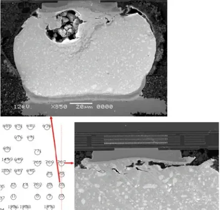
Figure 3 | A via region can be analyzed with a 3D electromagnetic model for return loss, insertion loss, and local structural change
5. Use These 6 Steps When Checking a High-Speed Layer Change
- Confirm the reference plane before the layer change. Do not only look at which layer the signal is on. Look at which GND or power plane it mainly references.
- Confirm the reference plane after the layer change. Whether the planes before and after are continuous and on the same net decides how the return can transition.
- Between the same GND reference layers, place a return ground via nearby first. The closer it is, the less the return current has to detour. Return structures next to a differential pair must also stay symmetric.
- When the reference changes from GND to a power plane, do not only add ground vias. The return must transition between two reference nets. Judge that with nearby decoupling capacitors and the actual stackup.
- Check whether the trace crosses a split, a ground gap, or a void in the reference plane. A ground via can only provide a vertical channel. It cannot automatically restore a reference plane that has already been cut.
- Finish with DRC, fabrication, and validation checks. Confirm via drill, pad, antipad, spacing, impedance, and fabricator capability together. Validate critical links with simulation, TDR, an eye diagram, or EMC testing.
6. What a Respin Review Should Ask Is Not "Was This Via Placed?"
On a high-speed board review, the useful evidence is not that the designer can recite "put a ground via next to a high-speed signal." It is that the forward path, the reference plane, and the return transition of that signal can be explained as one chain.
At a layer-change point, at least three questions should be answered:
- Which layer does the signal reference before and after the change? Map the stackup to the signal path first.
- Through what structure does the return current complete the vertical transition? A same-net ground via, or a decoupling path between reference planes?
- If this return via is removed, where does the current detour? The risk is understood only when the alternate path can be drawn.
Closing
The next time a high-speed signal changes layers, do not stare only at the signal via in the middle. Shift the view a little to the side: does the return current have a short path that can keep up with the signal?
Many EMC problems are not a wrong schematic and not a wrong chip. They come from seeing the signal during design and not seeing the complete current loop.