Separate solder wicking, via filling, and process confirmation first.
Via-in-pad is a process solution. It is not a geometric shortcut that Layout can decide on its own.

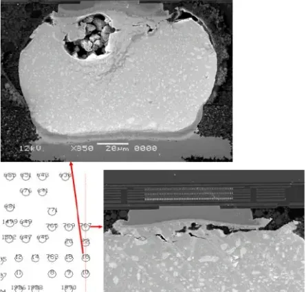
Figure 1 | Example of an open via-in-pad
An ordinary open via placed directly on a surface-mount pad can let molten solder migrate into the hole and change both the solder volume on the joint and the wetting balance at the two ends. Via-in-pad is not forbidden in every case, but it must be built with a filling, capping, surface-finish, and inspection flow accepted by the board shop and the assembly house.
As soon as component density rises, the most direct idea is to put the via in the pad: the route is shorter, fan-out saves space, and DRC may not even flag it.
The problem is that Layout only solves the electrical connection. Solder-paste printing, reflow wetting, solder wicking into the hole, surface flatness, and cost belong to another chain: fabrication and assembly.
The Joint Gives the First Warning: Why Solder Is Pulled Into the Hole
When a via lands on a surface-mount pad, solder can migrate into the hole and reduce the effective solder volume on the pad. On small pads or fine-pitch parts, a local change in solder volume more readily produces a poor joint, voiding, or inconsistent joints.
Small chip components also need balanced wetting force at both ends. If only one end has its thermal mass or solderable area changed by a via, reflow can create a shift or tombstoning risk.
BGAs Also Place Vias in Pads. The Difference Is in the Process
Fine-pitch BGA fan-out space is limited, so via-in-pad may become a necessary option. The key phrase is not "the via was put in." It is whether the via received matching fill, cap, and planarization.

Figure 2 | Example of via-in-pad placement on a BGA
An untreated drilled hole, a resin-filled and capped hole, and a microvia do not share the same manufacturing path or assembly risk. The project must write the structure name, hole-size capability, surface flatness, and acceptance requirements into the fabrication package.
On a Thermal Pad, the Soldering Window Is What Is Most Often Missed
The source document includes a case with vias inside a thermal pad. Thermal vias can help move heat into inner layers or the backside, but the openings also affect stencil aperture, solder migration, and void distribution.

Figure 3 | Example of a via array in a large pad
Thermal-via count and location must therefore be confirmed together with the package recommendation, board-shop capability, stencil plan, and assembly validation. Do not conclude from "more vias dissipate more heat" alone.
Give the Answer to the Board Shop, the Assembler, and Acceptance Evidence
- Confirm whether the component package allows or recommends via-in-pad.
- Distinguish the actual structure: ordinary through-hole, microvia, filled and capped via, and similar constructions.
- Have the PCB fabricator confirm hole size, fill, planarization, and surface-finish capability.
- Have the assembly house confirm the stencil, reflow, and solder-joint inspection plan.
- On prototype boards, verify joint quality with X-ray, cross-section, or another applicable process inspection.

Figure 4 | Comparison of a via at the pad edge and fan-out outside the pad
Three Common Judgments, Taken Apart
- "DRC did not flag it, so it can be built": electrical rules cannot replace soldering and manufacturing review.
- "Every via-in-pad is the same": via type, fill, and capping set the process boundary.
- "A thermal pad can be drilled at will": stencil design, solder migration, and voiding must be controlled at the same time.
Engineering judgment: via-in-pad is a process choice that crosses Layout, PCB fabrication, and SMT assembly. Only when the structure, the process, and the acceptance criteria are all confirmed is it a solution rather than a risk hidden inside the pad.
Conclusion: A Via Can Enter the Pad, but It Cannot Skip the Process
When space is tight, via-in-pad can be discussed. Routing convenience alone must not decide it.
The next time via-in-pad appears, ask first how the via will be processed, who can build it, and how it will be accepted. Ask whether it can be placed only after that.