PCB withstand voltage, commonly verified through a high-potential (Hi-Pot) test, is a key indicator of electrical safety and reliability. It evaluates whether the insulation system can withstand a specified voltage without breakdown, flashover, or other evidence of insulation failure.
PCB insulation performance is generally considered in two dimensions: layer-to-layer withstand voltage and conductor-to-conductor withstand voltage. These two evaluations address different insulation structures and failure mechanisms, so they must be considered separately during PCB design and qualification.
Layer-to-Layer Withstand Voltage
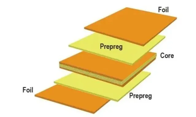
Layer-to-layer withstand voltage refers to the voltage that the insulating dielectric between different conductive layers can withstand. In a multilayer PCB, the dielectric system is formed primarily by materials such as FR-4, prepreg, and core laminate. Its performance is mainly determined by dielectric thickness, material properties, and manufacturing quality.
Material Properties
The dielectric breakdown strength of FR-4 is approximately 20–40 kV/mm. This value is a theoretical or material-level reference and is considerably higher than the voltage that should normally be used as a practical design limit. PCB designs must include substantial derating because the finished board contains material variations, interfaces, copper features, process tolerances, and possible manufacturing defects.
In other words, a laminate’s stated breakdown strength should not be treated as the allowable operating voltage of an actual PCB. Long-term reliability depends not only on the intrinsic strength of the resin system, but also on the uniformity of the dielectric, the quality of the lamination process, and the environmental conditions during operation.
Relationship Between Dielectric Thickness and Withstand Voltage
For engineering estimation, conventional FR-4 with a thickness of 1 mil is often considered capable of withstanding approximately 1,000 V DC in a bare-board instantaneous breakdown test. This value applies only to that specific test context and should not be interpreted as a general long-term operating-voltage limit.
When reinforced insulation is required, such as in some medical or other safety-critical applications, the required dielectric thickness may need to be approximately doubled. The actual requirement depends on the applicable product safety standard, insulation class, working voltage, environmental conditions, and qualification method.
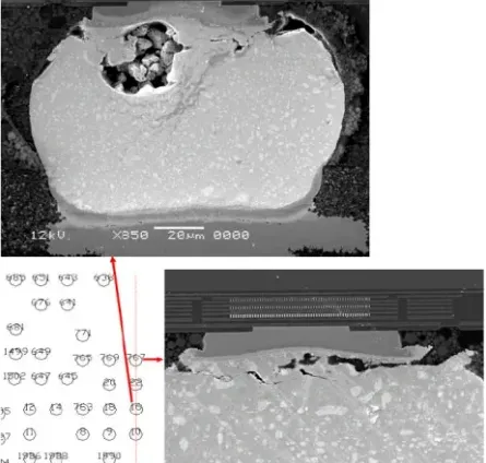
Thickness alone does not guarantee reliable insulation. Lamination voids, resin starvation, foreign particles, delamination, pinholes, and other process-related defects can significantly reduce the effective insulation strength. A defect within the dielectric can concentrate the electric field and become the starting point for partial discharge or eventual breakdown.
High-temperature and high-humidity environments also reduce the available insulation margin. For preliminary engineering consideration, an additional reduction of approximately 20–30% may be required under such conditions. The final derating value should be determined according to the actual material system, product requirements, and validation method rather than applied as a universal rule.
Conductor-to-Conductor Withstand Voltage
Conductor-to-conductor withstand voltage describes the insulation capability between conductive features, such as two traces or pads on the same PCB layer. Unlike layer-to-layer insulation, which is dominated by the dielectric between copper layers, conductor-to-conductor insulation is primarily determined by electrical clearance and creepage distance.
Electrical Clearance and Creepage Distance
Electrical clearance is the shortest straight-line distance through air between two conductive parts. Creepage distance is the shortest path along the surface of an insulating material between those conductors. Because moisture, dust, flux residue, and other contaminants can accumulate on a PCB surface, creepage distance is often greater than or equal to the required electrical clearance.
The appropriate surface spacing depends on several factors:
- Working voltage and the voltage waveform
- Pollution degree and the expected environmental contamination
- Insulation material and its comparative tracking index (CTI)
- Required insulation type
- Temperature, humidity, and other operating conditions
A contaminated or damp surface can provide a leakage path between conductors. Under sufficient voltage stress, this leakage path may develop into surface tracking, carbonization, or flashover. For this reason, conductor spacing cannot be selected solely from the nominal voltage value without considering the operating environment.

Design Standards and Initial Spacing Requirements
IPC-2221 can be used as an initial reference for PCB design. Its Table 6-1 specifies minimum electrical clearance values for different working-voltage ranges. Examples include approximately 0.1 mm at 30 V, 0.6 mm at 100 V, and 1.5 mm at 300 V.
These values provide a design starting point, but they do not automatically replace the product-level safety requirements applicable to the completed equipment. A final design may require larger spacing based on insulation classification, pollution degree, material group, environmental exposure, or certification requirements.
Insulation Type, Pollution Degree, and CTI
Product safety standards commonly distinguish between functional, basic, supplementary, double, and reinforced insulation. The required insulation performance increases progressively across these categories. A clearance or creepage distance that is adequate for functional insulation may not be sufficient for reinforced insulation.
Pollution degree is another important factor. The more severe the expected contamination, the greater the creepage distance normally needs to be. Dust and moisture can reduce surface resistance and increase the risk of leakage or tracking, particularly when the board is exposed to the surrounding environment.
Material group is related to the comparative tracking index, or CTI. A lower CTI indicates lower resistance to tracking, which generally results in a greater required creepage distance. Conventional FR-4 commonly has a CTI in the approximate range of 175–249 V, although the actual value depends on the specific laminate grade and manufacturer.
UL 796 specifies a withstand-voltage reference of 40 V/mil, or approximately 1.6 kV/mm. This value should be applied within the scope and test conditions of the relevant standard. It should not be confused with the required PCB trace spacing or used as a substitute for the complete product safety assessment.
The Role and Limitations of Solder Mask
Solder mask can provide additional surface insulation and may help improve the effective withstand performance between exposed conductors. However, it should not normally be treated as the only insulation barrier when calculating safety spacing.
Solder mask thickness and coverage can vary. Pinholes, cracks, contamination, edge coverage, adhesion problems, and mechanical damage may reduce its effectiveness. For safety-critical insulation, the primary design should therefore maintain appropriate copper-to-copper clearance and creepage distance even without relying exclusively on the solder mask.
Internal Insulation Between PCB Layers
The withstand voltage between copper layers depends on the dielectric strength of the PCB material and the thickness of the prepreg or core between those layers. For a typical 300 V withstand-voltage requirement, only a very thin resin layer may be sufficient from a purely physical breakdown-strength perspective. However, manufacturing tolerances and long-term reliability requirements lead to more conservative construction choices.
Compression variation during lamination, layer registration error, resin distribution, local thin areas, and pinhole defects can all reduce the effective insulation margin. For this reason, an internal dielectric thickness of at least 0.1–0.2 mm, approximately 4–8 mil, is often recommended for long-term electrical reliability in the stated design context.
For high-voltage applications, a laminate with a higher CTI may be appropriate. Additional protection can also be provided by applying conformal coating or potting material to the PCB surface. These coatings can reduce exposure to moisture and contamination and may allow a smaller external spacing requirement when the applicable safety evaluation permits it. They do not eliminate the need to verify the insulation system as a whole.
PCB Hi-Pot Testing
A Hi-Pot test is used to verify the insulation strength of a PCB or assembled product by applying a voltage that is substantially higher than the normal operating voltage. The purpose is to expose insulation weaknesses that may not appear during normal operation.
For PCB insulation evaluation, IPC-TM-650 2.5.7 is a key test reference. The exact test configuration, voltage, duration, connection method, and acceptance criteria must be defined for the product and insulation system under evaluation.

Test Voltage
The test voltage is normally much higher than the working voltage. A commonly used safety-design relationship is 2 × the working voltage + 1,000 V. For example, industrial-control and medical equipment may specify a requirement of at least 1,500 V AC for 60 seconds. This example is not a universal value; the applicable product standard and insulation category determine the actual test condition.
Test Duration
Typical Hi-Pot test durations are 30 or 60 seconds. Production-line testing may use a much shorter duration to support manufacturing throughput, provided that the shortened test method has been validated against the applicable qualification requirements.
Pass/Fail Criteria
During the specified test interval, the insulation must not experience dielectric breakdown or flashover. A failure may be indicated by an electrical arc, visible sparking, excessive leakage, or another condition defined by the test procedure. A board that passes a brief test is not automatically qualified for every operating environment; the test result is meaningful only when the voltage, duration, connection points, and acceptance criteria are properly specified.
Key Design Considerations
PCB withstand-voltage design requires a coordinated evaluation of material selection, dielectric thickness, electrical clearance, creepage distance, insulation type, contamination level, CTI, manufacturing capability, and environmental conditions. Layer-to-layer and conductor-to-conductor insulation should be reviewed independently because they involve different physical structures and failure paths.
IPC-2221 can serve as a practical starting point for PCB spacing and construction decisions. However, IEC, UL, and other applicable product-safety standards provide the binding requirements for equipment certification. A reliable design combines conservative spacing and dielectric selection with controlled fabrication, appropriate environmental protection, and a Hi-Pot test that reflects the actual safety requirements of the finished product.