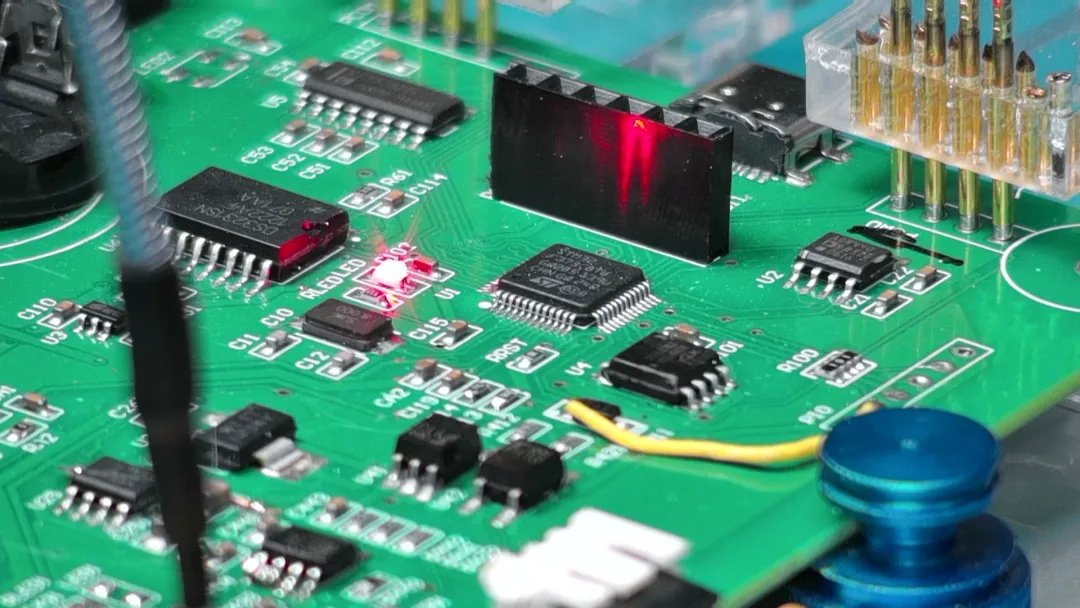
The 3W rule is an empirical guideline for PCB routing. It requires the center-to-center spacing between adjacent signal traces to be at least three times the width (W) of a single trace. For example, if the trace width is 6 mil, the center spacing should be at least 18 mil. The primary purpose is to reduce crosstalk between signals and maintain signal integrity (SI) and electromagnetic compatibility (EMC).

The 3W rule is one method of controlling crosstalk, but it should be treated as a design reference rather than an absolute requirement. In practical PCB design, applying 3W alone cannot guarantee that crosstalk will be eliminated.
Based on engineering practice, when no ground guard trace is used, signal traces may need to be separated by more than 1 cm to effectively suppress crosstalk in some situations. Therefore, the 3W rule should be applied selectively between noise-source signals, such as clock traces, and quiet signal traces. It is also useful between "dirty" traces that may be affected by EFT/B or ESD and "clean" traces that require protection. In these cases, designers may need both 3W spacing and a grounded guard trace or ground shielding.
Not every trace on a PCB must follow the 3W rule. Before routing, it is important to identify which traces genuinely require this spacing based on their edge rate, operating frequency, signal amplitude, sensitivity, routing length, and system requirements.
Why Three Times the Trace Width-
1. Reducing Electric-Field Coupling
Increasing the spacing between adjacent traces reduces the electric-field interaction between them. Engineering experience indicates that when the center-to-center spacing reaches 3W, approximately 70% of the electric-field coupling between the traces can be suppressed, significantly reducing the risk of crosstalk.
For this reason, the 3W rule is often described as a practical spacing guideline: when the center spacing is no less than three times the trace width, approximately 70% of the electric-field interaction is avoided. If a higher level of isolation is required, a 10W rule may be used as a reference, corresponding to approximately 98% isolation in the simplified relationship described by this guideline.
These percentages should not be interpreted as universal guarantees. The actual coupling level also depends on the PCB stackup, trace geometry, dielectric thickness, reference-plane distance, parallel routing length, signal rise time, and termination conditions.
2. Controlling Magnetic-Field Coupling
A 3W spacing also helps reduce mutual inductive coupling and magnetic-field interference, particularly for high-frequency signals. Magnetic coupling is generated by the mutual inductance between signal loops. Its strength is affected by several factors:
- Spacing (d): As the center-to-center distance between conductors increases, mutual inductance decreases.
- Signal frequency (f): Magnetic-field coupling becomes more significant as the frequency content of the signal increases.
- Loop area (A): The larger the loop formed by a signal and its return path, the stronger the mutual inductive coupling can become.
In practical PCB design, trace spacing should therefore be considered together with return-path continuity. Increasing the distance between two traces is helpful, but a poorly controlled return path can still produce a large current loop and increase electromagnetic coupling.
The simplified mutual-inductance formula is shown below:
3. A Balance Between Engineering Practice and Electromagnetic Theory
The 3W value originates from a combination of engineering practice and electromagnetic-field theory. It provides a practical compromise between routing density and signal quality. Excessive spacing consumes valuable PCB area, while insufficient spacing increases capacitive and inductive coupling. The 3W guideline offers a simple starting point for managing this tradeoff when a detailed crosstalk analysis is not available.
However, the required spacing around vias and other discontinuities must be evaluated carefully. For example, a via located between two traces may be connected to a third trace that carries a signal susceptible to electromagnetic interference. Examples include reset signals, audio or video traces, analog-control traces, and I/O interface traces. The via can receive additional coupled energy through either capacitive or inductive coupling.
To minimize crosstalk from a trace to the via, the spacing calculation should include the via diameter and the required clearance around the via. Within a distance of 2W from a clock trace, no unrelated signal should be placed. A similar spacing requirement can be applied around traces carrying substantial RF energy, because RF energy may couple into nearby component pins.
Must Every PCB Satisfy the 3W Rule-
In real PCB layouts, maintaining 3W spacing everywhere is often impractical. The first step is to identify the signals that require strict spacing control. High-speed signals and signals with fast rise times are usually more sensitive to crosstalk. In contrast, many GPIO, I2C, and UART traces may not require such a large clearance when their operating conditions and system margins permit a smaller spacing.


For example, more routing space can be allocated to MIPI signals, while low-speed interfaces and GPIO-level signals can be routed using the minimum spacing permitted by the manufacturing process. This approach reserves routing resources for signals that are more likely to affect system performance.
Crosstalk is generally acceptable if it does not interfere with normal product operation. The actual requirement depends on the application, interface, signal amplitude, noise margin, and compliance criteria. Different interfaces can therefore have very different crosstalk limits.
For example, USB 3.0 specifications define cable crosstalk requirements. These requirements distinguish between crosstalk within SuperSpeed pairs and crosstalk between SuperSpeed signals and the D+/D- pair.
Because USB has a relatively clear structure and a limited number of signals, its crosstalk requirements are comparatively straightforward. For higher-speed buses or interfaces with tighter margins, crosstalk evaluation becomes more complicated. One parameter used for this purpose is integrated crosstalk noise (ICN).
For example, the OIF CEI requirements cited here specify an integrated crosstalk noise level below 3.9 mV. The MDNEXT value should be below 1.35 mV RMS, and the MDFEXT value should be below 3.6 mV RMS.
The following image illustrates an example of crosstalk calculation:
These values and formulas are examples of formal crosstalk evaluation. Detailed calculations should follow the applicable CEI requirements. In many projects, engineers do not calculate every parameter manually. Instead, the interface specification, simulation tools, and compliance criteria provide the required limits.
When no special crosstalk requirement is specified, a commonly used engineering reference is to limit crosstalk to approximately 5% of the signal amplitude or supply voltage, equivalent to approximately -26 dB. When the signal amplitude or supply voltage is small, a tighter target such as 1% or -40 dB may be used. These values are calculation references rather than universal rules.
The final evaluation must consider the actual design. Crosstalk depends not only on the physical transmission structure but also on signal behavior, including the aggressor rise time, the relative phase between the aggressor and victim signals, the parallel coupling length, and the characteristics of the receiving circuit.
What to Do When the 3W Rule Cannot Be Met
When routing density prevents 3W spacing, several other design techniques can be combined to reduce crosstalk:
- Use ground isolation.
- Insert a ground guard trace between critical signal traces so that the ground potential can absorb part of the coupled interference.
- For a high-speed clock trace, use a grounded guard trace or a row of ground vias where appropriate.
- Optimize the layer stackup.
- Route signals on adjacent layers in orthogonal directions, such as horizontal routing on one layer and vertical routing on the next, to reduce broadside coupling.
- Use ground layers as shields. A signal-ground-signal layer arrangement can provide better isolation between signal layers.
- Use differential signaling.
- High-speed interfaces such as USB and HDMI can use differential pairs. Their common-mode rejection and balanced routing characteristics can reduce sensitivity to external interference, although differential routing does not eliminate the need for appropriate spacing and reference-plane control.
- Apply termination and impedance matching.
- Series termination resistors or parallel termination resistors can reduce signal reflections and therefore reduce the signal's sensitivity to coupled noise.
- Sacrifice routing density locally.
- Give priority to high-frequency and sensitive signals. Spacing can be relaxed for low-frequency or noncritical signals when the resulting crosstalk remains within the system margin.
- Verify the design with simulation.
- Use SI/PI tools such as HyperLynx or Sigrity to estimate crosstalk and determine whether an exception to the 3W rule is acceptable.
Crosstalk Control Requires More Than Increasing Spacing
Because PCB area is limited, crosstalk cannot always be controlled simply by separating every trace by 3W. Placement, stackup selection, return-path design, routing topology, termination, and filtering must be considered together.
- Group logic devices according to their functions and keep the bus topology under tight control.
- Minimize the physical distance between components to reduce trace length and coupling exposure.
- Keep high-speed traces and components, such as crystal oscillators, away from I/O interconnects and other areas that are susceptible to noise and coupling.
- Provide appropriate termination for high-speed traces.
- Avoid long, parallel trace runs. Provide sufficient spacing to reduce inductive coupling and shorten the parallel-coupling length whenever possible.
- Route traces on adjacent layers orthogonally, particularly for microstrip and stripline structures, to reduce interlayer capacitive coupling.
- Reduce the distance between signal traces and their reference planes. A closer reference plane provides a tighter return path and can reduce the effective loop area.
- Separate high-noise sources, such as clocks, I/O, and high-speed interconnects. Different signal groups can be assigned to different layers when the stackup supports this approach.
- Increase the spacing between signal traces whenever possible to reduce capacitive crosstalk.
- Reduce lead inductance and avoid combining extremely high-impedance or extremely low-impedance loads with sensitive circuits without evaluating the consequences. High-impedance loads can increase the voltage generated by capacitive crosstalk, while very low-impedance loads can involve higher current and increase the effect of inductive crosstalk. For analog circuits, a relatively stable load impedance in the range of 10 Ω to 10 kΩ is cited as an engineering reference.
- Route high-speed periodic signals on internal PCB layers whenever possible to reduce radiation and susceptibility to external fields.
- Use impedance matching to maintain signal integrity and limit overshoot.
- For signals with fast rise times, such as those with a rise time of less than 3 ns, apply additional crosstalk-control measures such as ground shielding. Signals susceptible to EFT/B or ESD and lacking adequate filtering can be routed near the PCB edge when the system layout requires it.
- Use a continuous ground plane whenever possible. Compared with a trace without an effective ground plane, a signal referenced to a ground plane is cited as achieving approximately 15–20 dB of attenuation.
- Apply ground shielding around high-frequency or sensitive traces. On a two-layer board, ground shielding is cited as providing approximately 10–15 dB of attenuation.
- Use balanced lines, shielded cables, or coaxial cables when the interconnect application requires additional isolation.
- Apply filtering to interfering signal lines and sensitive signal lines.
- Optimize the layer assignment and routing geometry. Increasing the trace-to-trace spacing, shortening parallel runs, reducing the distance between signal layers and reference planes, and reducing the signal-to-plane spacing can all help reduce crosstalk.
Conclusion
The 3W rule has a practical basis in the reduction of electric-field and magnetic-field coupling. It is useful as an initial PCB routing guideline, especially for high-speed, fast-edge-rate, RF, clock, and noise-sensitive signals. However, it is not a universal pass/fail requirement for every trace.
A sound design process identifies the signals that require stricter isolation, assigns routing space according to actual risk, and combines spacing with continuous reference planes, controlled return paths, appropriate layer transitions, termination, shielding, filtering, and SI simulation. The correct spacing is ultimately determined by the signal behavior, coupling structure, interface margin, and system-level performance requirements—not by the 3W number alone.