


PCB Manufacturing
Printed Circuit Boards (PCBs) form the backbone of modern electronics, serving as the essential platform where components connect to create functional devices. In the PCB Manufacturing category, readers gain access to a comprehensive collection of resources designed to demystify the intricate processes involved in producing these critical elements. From initial design considerations to final assembly and testing, this category covers every stage, providing valuable insights for engineers, hobbyists, and industry professionals alike. Understanding PCB manufacturing is crucial for anyone involved in electronics development. This field encompasses a wide range of topics, including material selection, such as FR-4 substrates and advanced laminates, as well as fabrication techniques like etching, drilling, and soldering. Articles here delve into best practices for optimizing layouts to minimize signal interference, ensuring reliability in high-stakes applications. Tutorials guide users through prototyping methods, while in-depth analyses explore emerging trends like flexible PCBs and additive manufacturing, which are revolutionizing industries from consumer gadgets to aerospace systems. The practical value of mastering PCB manufacturing extends to real-world scenarios, where efficient production can reduce costs, enhance performance, and accelerate time-to-market. For instance, insights on multilayer board construction help in designing compact devices for IoT applications, and discussions on quality control standards prevent common pitfalls in mass production. By engaging with the diverse guides and expert perspectives in this category, readers can build a solid foundation in PCB technologies, apply proven strategies to their projects, and stay ahead in an ever-evolving field. Whether troubleshooting assembly issues or exploring sustainable manufacturing practices, the knowledge shared here empowers informed decision-making and innovation in electronics.
Latest Blogs
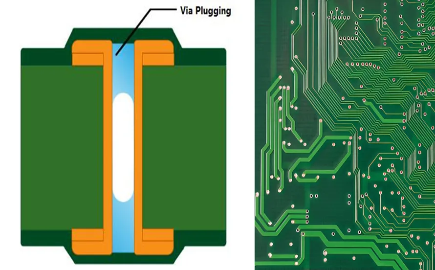
Boosting PCB Reliability: How Via Filling Prevents Solder Wicking and Contamination
Discover how via filling prevents PCB wicking during BGA assembly. Learn proven techniques to eliminate solder wicking, reduce contamination, strengthen joints, and improve high-density PCB reliability per IPC standards.
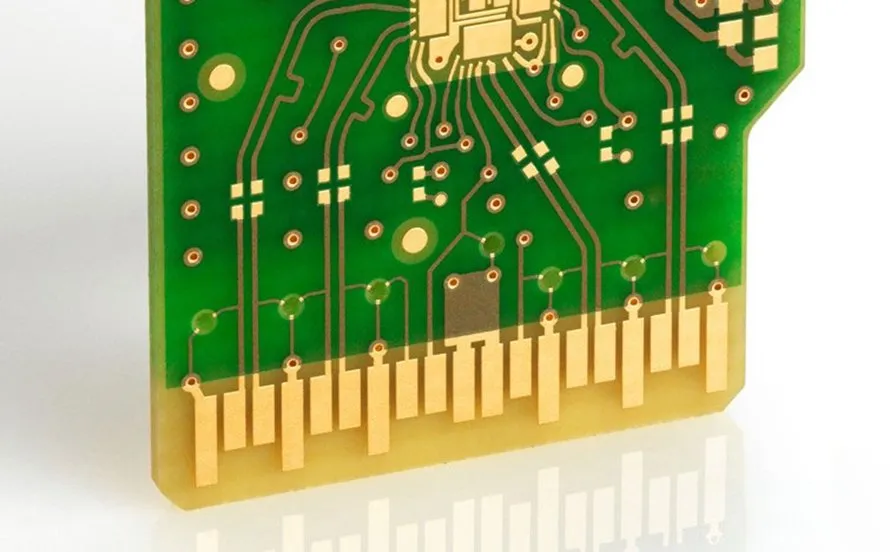
Mastering PCB Gold Finger Insertion and Extraction: Techniques for Prolonging Connector Life
Proper PCB insertion techniques prevent damage to gold fingers and extend connector life. Covers extraction tools for PCBs, cleaning gold fingers for better contact, reducing friction on gold fingers, and best practices for hobbyists to ensure reliable performance over many cycles.
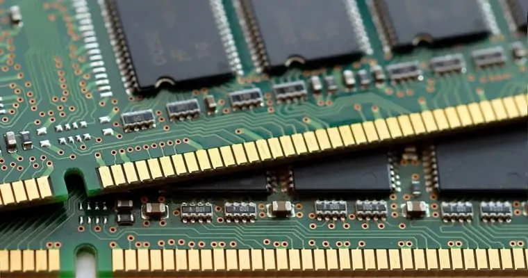
PCB Gold Finger Design Rules: Avoiding Common Pitfalls for Reliable Connections
PCB gold finger design rules address spacing, length, alignment, chamfer, keepout areas for gold fingers, and plated through holes near gold fingers. Avoid pitfalls like misalignment and plating defects for reliable edge connectors. Practical tips help electric engineers ensure durable performance in high cycle applications.
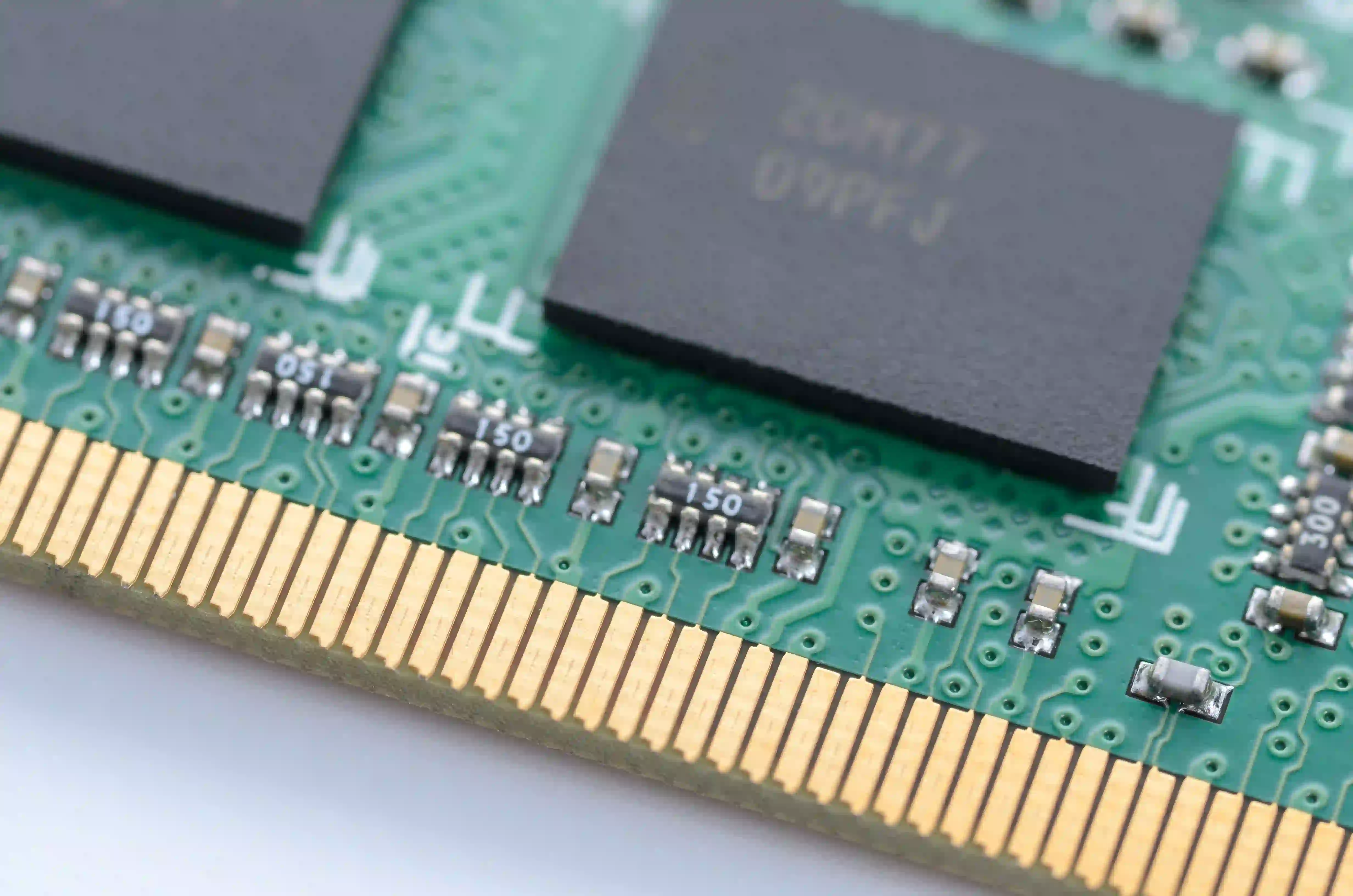
Selective Gold Plating for PCBs: A Comprehensive Cost Analysis and Application Guide
Compare selective gold plating vs full board plating costs for PCBs in connectors and high-wear areas. This guide details masking techniques, applications, and factors affecting pricing to help electric engineers balance performance and budget effectively.

The Impact of Solder Mask on PCB Gold Finger Performance: Best Practices
Solder mask clearance for gold fingers prevents encroachment, protects signal integrity, guides material selection, and stops solder bridging in PCBs. Electric engineers find practical design rules, fabrication tips, and standards like IPC-6012E for reliable edge connector performance and high mating cycles.
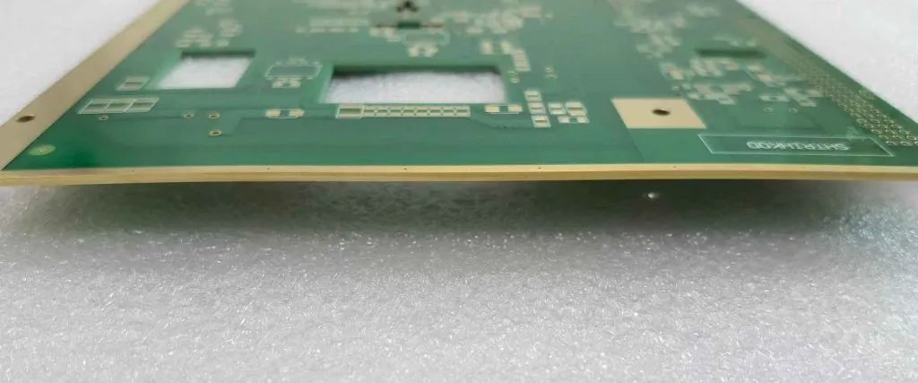
The Role of PCB Edge Plating in Board to Board Connections
PCB edge plating board to board connections support modular electronics with strong electrical and mechanical links. Details cover technical principles, design guidelines, assembly processes per IPC-6012E and J-STD-001, troubleshooting for voids and warpage, plus best practices for electrical engineers building reliable systems.
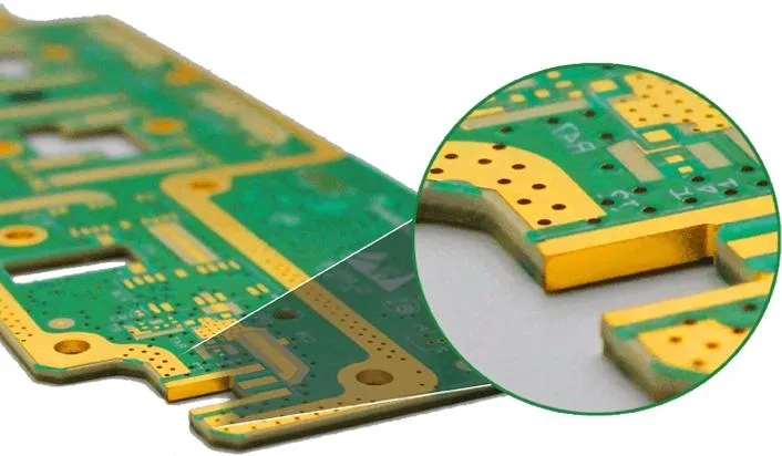
PCB Edge Plating for Enhanced EMC Performance: A Practical Guide
Discover how PCB edge plating creates a continuous conductive barrier to reduce edge radiation, improve shielding, and achieve superior EMC compliance in high-speed designs. Learn practical implementation tips, design rules, and troubleshooting for reliable results.
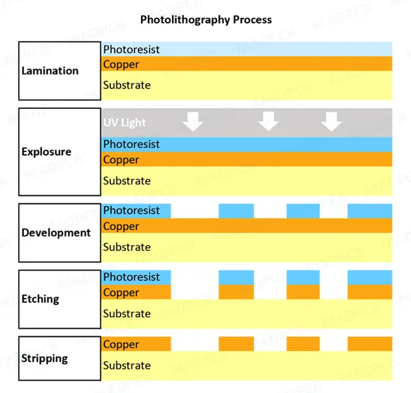
PCB Direct Imaging: Overcoming Challenges with Warped or Uneven Substrates
Warped substrates disrupt PCB direct imaging by causing focus errors and yield drops in LDI processes. Apply vacuum fixturing, dynamic focusing, and lamination controls to flatten panels and ensure precise exposure. Tackle PCB manufacturing challenges with standards-based practices for better results and higher throughput.
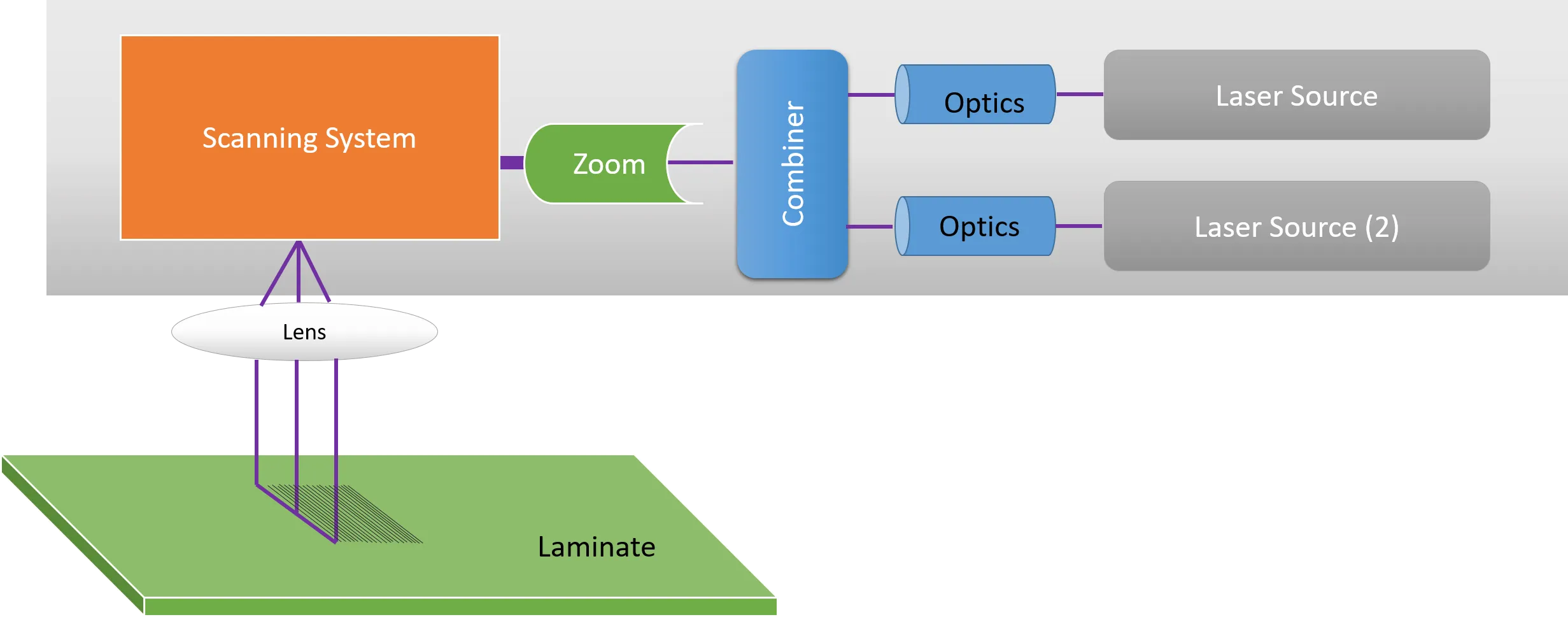
Automating PCB Direct Imaging: Integrating LDI into Your Production Line
Integrate LDI into PCB production lines for automated PCB direct imaging. Covers technical principles, workflow steps, best practices, troubleshooting, and benefits for higher yields in PCB manufacturing automation and smart factory environments. Ideal for electric engineers.
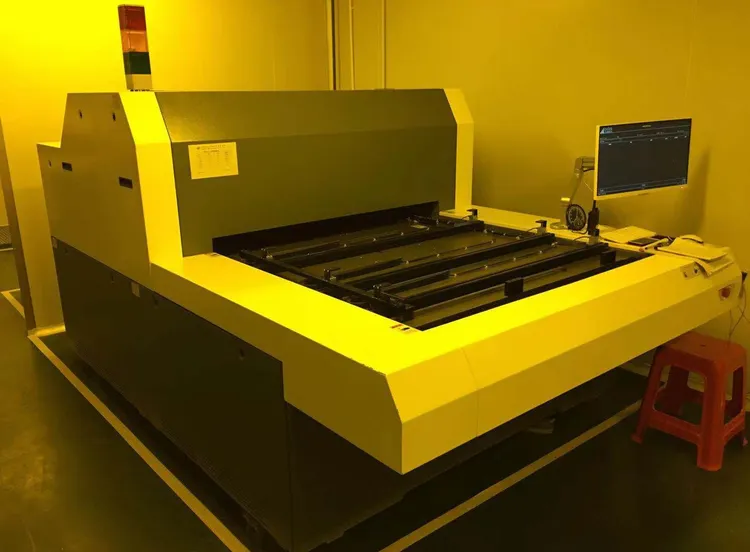
PCB Direct Imaging for High Reliability Applications: Aerospace and Medical
PCB direct imaging with LDI delivers precision for high-reliability aerospace and medical PCBs, enabling fine features and multilayer alignment per IPC-6012E standards. This guide covers technical principles, sector applications, best practices, and quality controls for engineers facing stringent requirements.
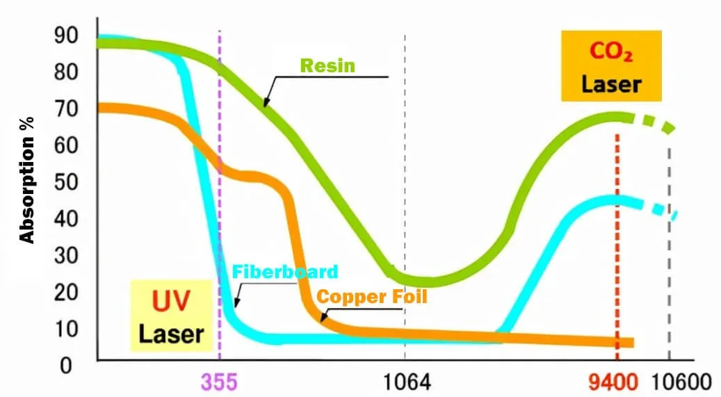
HDI PCB Laser Drilling: Materials, Techniques, and Equipment
HDI PCB laser drilling materials like FR-4 and polyimide support HDI boards with precise techniques such as CO2 and UV ablation. Essential HDI PCB equipment features galvo scanners and vision systems. Factory insights cover best practices, troubleshooting, and IPC standards for electric engineers seeking reliable manufacturing.
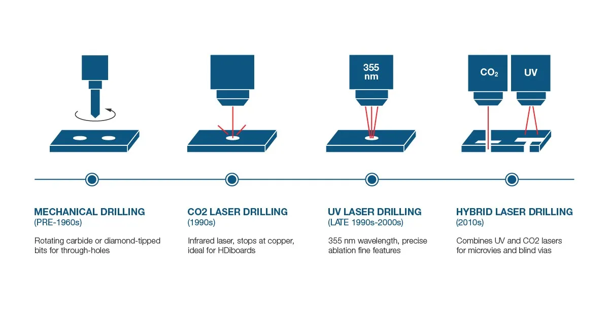
PCB Laser Drilling: How it Works, Benefits, and Applications
PCB laser drilling process creates precise microvias for HDI PCBs. Key benefits include superior density cleaner holes and no mechanical stress. Applications cover smartphones automotive and medical devices plus best practices and standards for manufacturing.


