


PCB Manufacturing
Printed Circuit Boards (PCBs) form the backbone of modern electronics, serving as the essential platform where components connect to create functional devices. In the PCB Manufacturing category, readers gain access to a comprehensive collection of resources designed to demystify the intricate processes involved in producing these critical elements. From initial design considerations to final assembly and testing, this category covers every stage, providing valuable insights for engineers, hobbyists, and industry professionals alike. Understanding PCB manufacturing is crucial for anyone involved in electronics development. This field encompasses a wide range of topics, including material selection, such as FR-4 substrates and advanced laminates, as well as fabrication techniques like etching, drilling, and soldering. Articles here delve into best practices for optimizing layouts to minimize signal interference, ensuring reliability in high-stakes applications. Tutorials guide users through prototyping methods, while in-depth analyses explore emerging trends like flexible PCBs and additive manufacturing, which are revolutionizing industries from consumer gadgets to aerospace systems. The practical value of mastering PCB manufacturing extends to real-world scenarios, where efficient production can reduce costs, enhance performance, and accelerate time-to-market. For instance, insights on multilayer board construction help in designing compact devices for IoT applications, and discussions on quality control standards prevent common pitfalls in mass production. By engaging with the diverse guides and expert perspectives in this category, readers can build a solid foundation in PCB technologies, apply proven strategies to their projects, and stay ahead in an ever-evolving field. Whether troubleshooting assembly issues or exploring sustainable manufacturing practices, the knowledge shared here empowers informed decision-making and innovation in electronics.
Latest Blogs
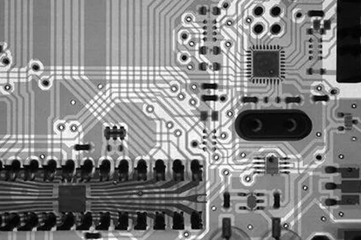
X Ray Inspection For Prototype PCB Rework
Learn how X-ray inspection for prototype PCB rework reveals hidden defects like voids, bridges, and head-in-pillow failures in BGAs and QFNs. This guide covers technical principles, integration into NPI workflows, IPC J-STD-001 compliance, best practices, and troubleshooting to reduce iterations and accelerate time-to-market.
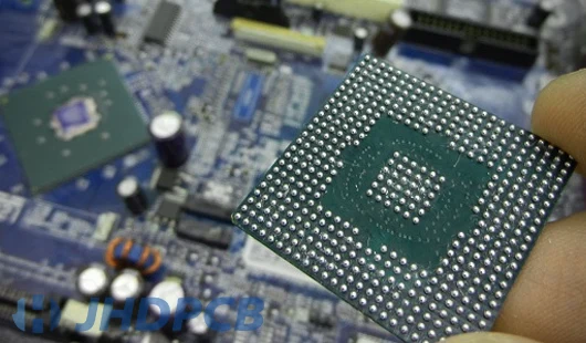
BGA Reballing: Prototype PCB Rework Process
Learn what BGA reballing is, how the BGA reballing process works, and best practices for ball grid array rework, BGA assembly, inspection, and repair.
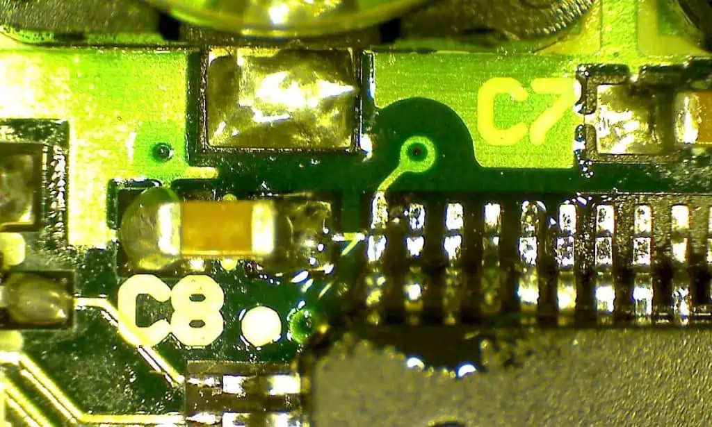
Step by Step: Manual PCB Cleaning After Rework for Optimal Results
Follow this detailed step-by-step manual PCB cleaning after rework guide to remove flux residues, prevent corrosion, and ensure reliability. Learn solvent selection, safe techniques, cleanliness testing (ROSE, ion chromatography), and IPC-compliant best practices for high-reliability electronics.
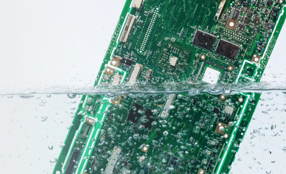
PCB Cleaning Equipment for Rework: A Buyer's Guide
Discover the best PCB cleaning equipment for rework in this buyer's guide. Compare ultrasonic cleaners, spray-in-air systems, benchtop stations, and manual tools. Key buying considerations, best practices, and troubleshooting for reliable flux removal and IPC compliance.
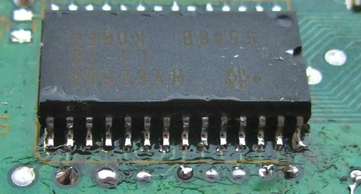
Troubleshooting Common PCB Cleaning Problems After Rework
Tackle white residue after PCB cleaning, sticky residue after rework cleaning, and stubborn flux removal with practical steps for electric engineers. Learn causes, IPA methods, ultrasonics, drying techniques, and IPC standards to ensure clean, reliable PCB assemblies and avoid failures.
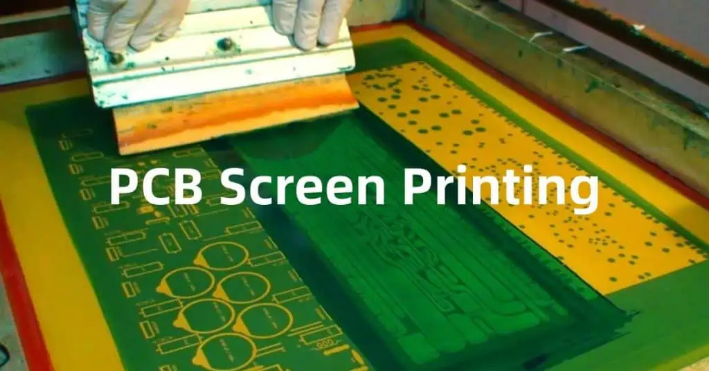
Silkscreen Placement: Optimizing Space in Compact PCB Designs
Compact PCB silkscreen tips minimize footprint for tight spaces placement. Prioritize designators, pad clearances, label grouping. IPC standards ensure legibility and assembly efficiency in high-density boards. Includes best practices, troubleshooting, and FAQs for engineers.
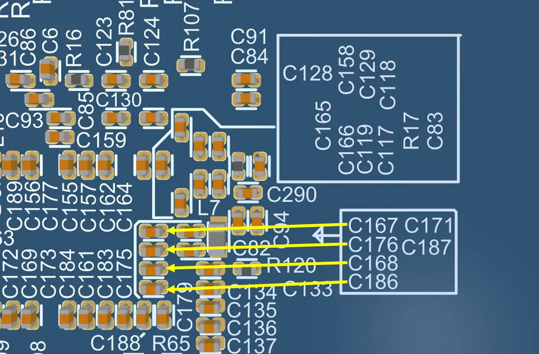
The Essential Guide to Silkscreen Design with Altium Designer
Get step-by-step instructions on Altium silkscreen layer setup, creating silkscreen markings in Altium, and importing logos into Altium silkscreen. This guide helps electric engineers design clear PCB overlays for better assembly, compliance, and troubleshooting in PCB layouts.
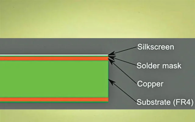
Silkscreen Design for Multi Layer PCBs: Best Practices and Considerations
Discover expert silkscreen design best practices for multi-layer PCBs. Learn placement strategies, inner-layer myths, overlap avoidance, visibility tips, and troubleshooting to ensure error-free assembly and superior manufacturability.
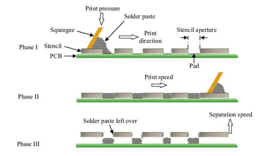
Why is My Solder Paste Drying Out? Common Causes and Prevention Tips
Solder paste drying out affects PCB assembly quality and yield. Learn common causes like improper storage, air exposure, and temperature changes, plus practical tips for storing solder paste, handling, and avoiding dry solder paste issues for better SMT performance.
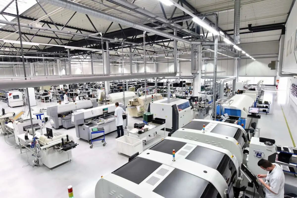
Safe Handling Practices for Solder Paste: Protecting Yourself and the Environment
Learn essential solder paste safety practices including PPE selection, proper refrigerated storage, spill response, MSDS interpretation, and compliant disposal methods to protect workers and the environment in PCB manufacturing.

Void Formation in PCB Lamination: Understanding the Mechanisms and Mitigation Strategies
PCB lamination voids arise from air pockets, material outgassing, and process flaws in manufacturing. This guide details formation mechanisms, detection methods, and proven fixes like vacuum lamination, pre-baking, and press optimization for stronger boards and higher yields.
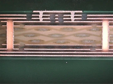
Delamination in PCB Lamination: Causes, Detection, and Prevention
Discover the primary causes of delamination in PCB lamination, effective detection techniques like ultrasonic testing and cross-sectioning, and proven prevention strategies including moisture control and optimized process parameters. Reduce defects and improve multilayer PCB reliability with expert manufacturing insights.


