


PCB Manufacturing
Printed Circuit Boards (PCBs) form the backbone of modern electronics, serving as the essential platform where components connect to create functional devices. In the PCB Manufacturing category, readers gain access to a comprehensive collection of resources designed to demystify the intricate processes involved in producing these critical elements. From initial design considerations to final assembly and testing, this category covers every stage, providing valuable insights for engineers, hobbyists, and industry professionals alike. Understanding PCB manufacturing is crucial for anyone involved in electronics development. This field encompasses a wide range of topics, including material selection, such as FR-4 substrates and advanced laminates, as well as fabrication techniques like etching, drilling, and soldering. Articles here delve into best practices for optimizing layouts to minimize signal interference, ensuring reliability in high-stakes applications. Tutorials guide users through prototyping methods, while in-depth analyses explore emerging trends like flexible PCBs and additive manufacturing, which are revolutionizing industries from consumer gadgets to aerospace systems. The practical value of mastering PCB manufacturing extends to real-world scenarios, where efficient production can reduce costs, enhance performance, and accelerate time-to-market. For instance, insights on multilayer board construction help in designing compact devices for IoT applications, and discussions on quality control standards prevent common pitfalls in mass production. By engaging with the diverse guides and expert perspectives in this category, readers can build a solid foundation in PCB technologies, apply proven strategies to their projects, and stay ahead in an ever-evolving field. Whether troubleshooting assembly issues or exploring sustainable manufacturing practices, the knowledge shared here empowers informed decision-making and innovation in electronics.
Latest Blogs
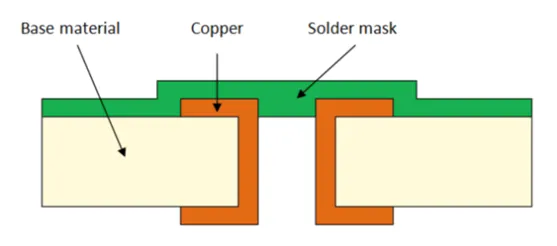
PCB Via Plating: Process, Methods, and Thickness Requirements
Learn how PCB via plating works, compare via plating methods, understand copper plating thickness requirements, and improve through-hole coverage and PCB reliability with practical manufacturing insights from AIVON.
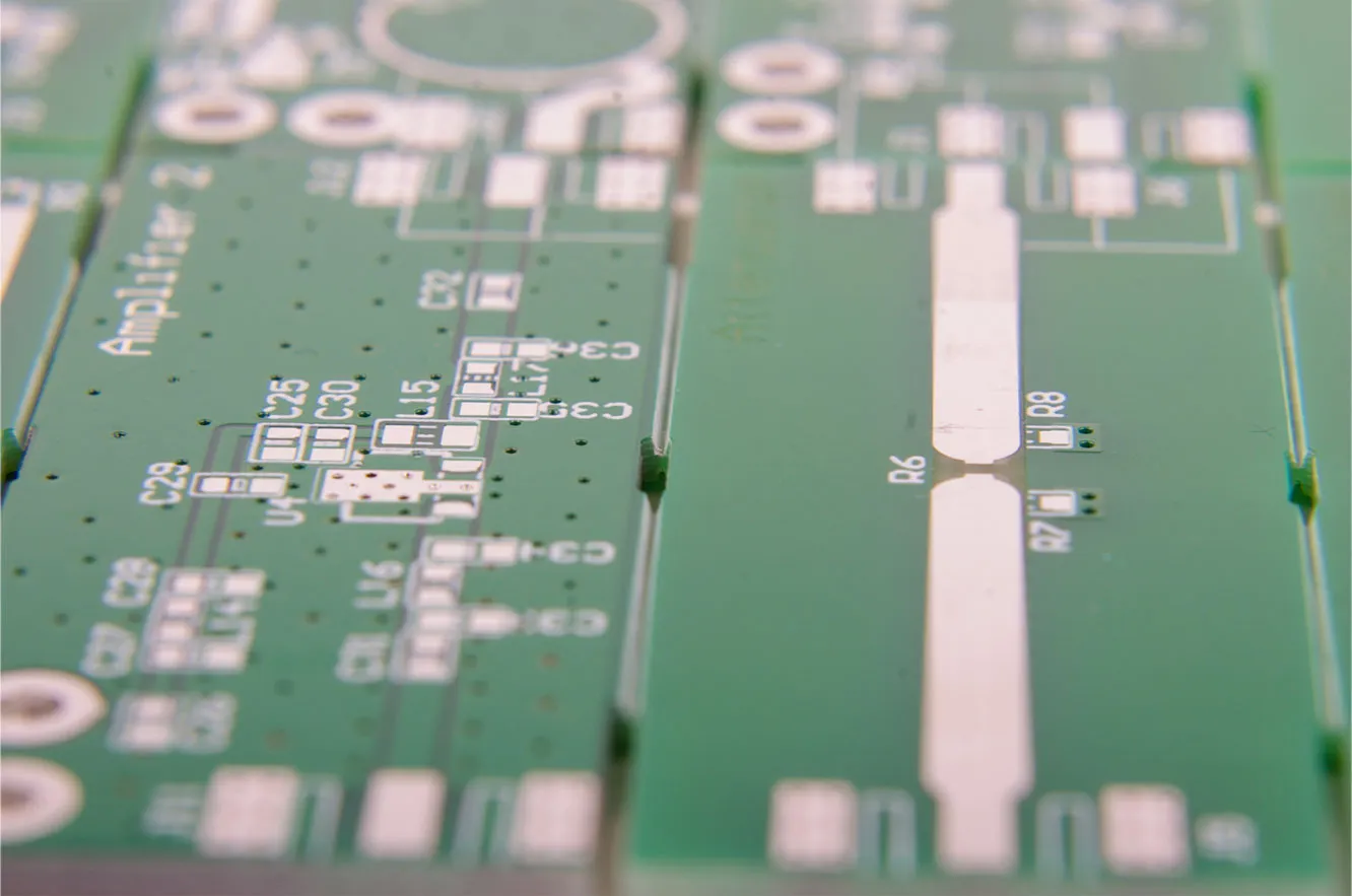
Cracking the Code: Optimizing V Scoring for PCB Depaneling Success
Master optimizing V-scoring for reliable PCB depaneling. Learn V-score design rules, residual web tolerances, stress reduction techniques, IPC-2221 guidelines, and practical tips to maximize material utilization while minimizing microcracks and warpage.
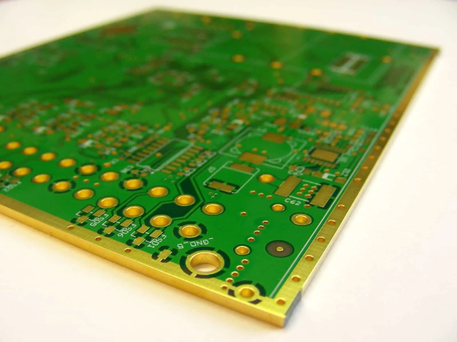
Choosing the Right Materials for PCB Edge Plating
Learn how to choose the right PCB edge plating materials including copper base layers, ENIG finish, hard gold, and immersion silver. This guide covers properties, design rules, IPC standards, cost-performance trade-offs, and manufacturing best practices for reliable edge connectors and EMI shielding.
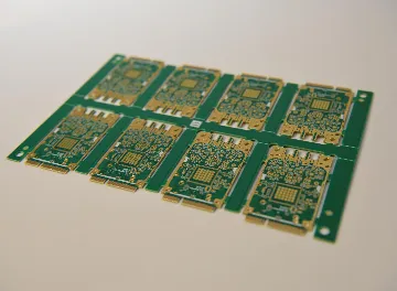
Router Depaneling: The Go To Method for Intricate PCB Designs?
PCB router depaneling suits intricate PCB designs by milling complex paths cleanly on routing machines. Details cover bit selection for durability, dust collection to avoid contamination, speed settings for quality, and automation for volume production. Get practices for sharp edges and reliable yields.
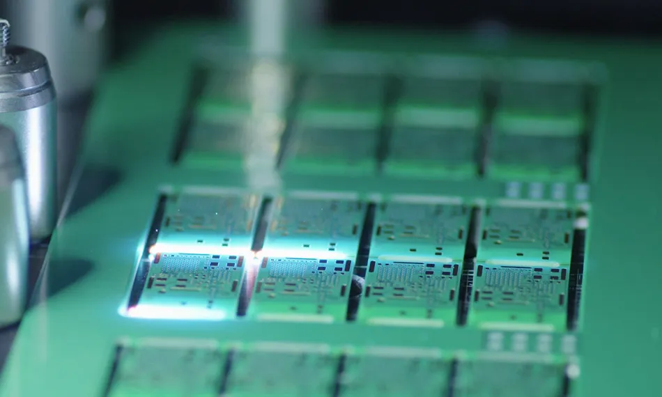
Laser PCB Depaneling: Achieving High Precision and Minimal Stress
Laser PCB depaneling provides precise cuts with minimal stress, outperforming mechanical methods like routing. This guide covers technical principles, stress comparisons, flex PCB applications, equipment selection, costs, and best practices for reliable manufacturing and higher yields.
The Future of Electronics: Why High Tg PCBs are Essential
High Tg PCBs maintain stability in high heat for reliable electronics. This article covers High Tg PCB market trends, technology roadmap, innovations, applications in automotive and aerospace, plus best practices for electric engineers on design, fabrication, and assembly to prevent failures.

High Tg PCB Manufacturing for High Speed Digital Circuits
High-Tg PCB manufacturing ensures signal integrity in high-speed digital circuits through stable dielectric constant, low signal loss, precise impedance matching, and strong high-frequency performance. Factory best practices and troubleshooting tips help electric engineers produce reliable boards for demanding applications.
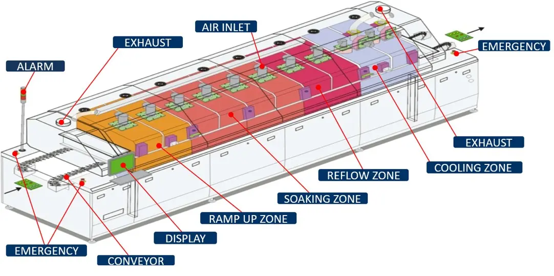
High Tg PCB Assembly: Best Practices for High Temperature Soldering
Follow best practices for High-Tg PCB assembly and high-temperature soldering, covering reflow profiles, solder paste selection, component placement, and process steps. Minimize warpage, voids, and defects for reliable performance in demanding electronics.
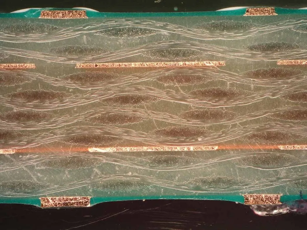
High Tg PCB Manufacturing: Design Tips for Optimal Performance
Electrical engineers gain practical High Tg PCB design rules, layer stackup guidelines, via strategies, impedance control methods, and signal integrity practices for reliable manufacturing. Prevent warpage, ensure thermal stability, and boost performance in demanding applications with factory insights.
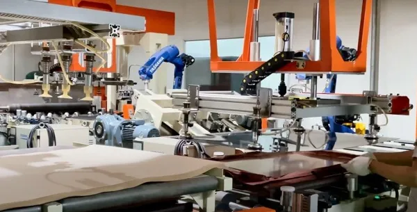
Heavy Copper PCBs for Aerospace: Enhancing Reliability in Extreme Environments
Thick copper PCB for aerospace stands out in high-reliability PCB design by handling extreme thermal stress, vibration, and power demands. This article covers engineering principles, manufacturing challenges, thermal stress testing methods, and best practices for robust avionics and satellite boards.
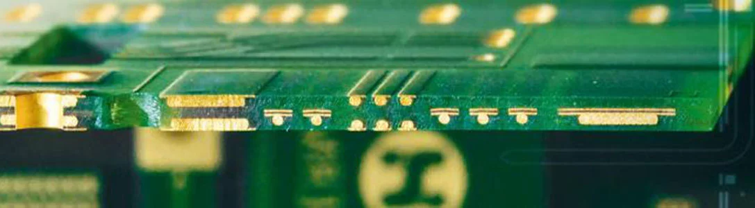
Thick Copper PCB Manufacturing for Electric Vehicle (EV) Applications
Discover how thick copper PCB manufacturing powers electric vehicles with superior current handling, thermal management, and reliability. From BMS to EV chargers – design, process, and standards explained.
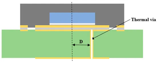
Thick Copper PCBs: The Secret to Efficient Heat Dissipation in LED Lighting
Thick copper PCBs handle heat dissipation in high-power LED lighting effectively. Details on thermal vias in thick copper PCB, high power LED PCB design, aluminum vs thick copper PCB trade-offs, and LED PCB manufacturing process guide engineers to reliable designs and performance.


