In one consumer-electronics project, a first production run of 500 PCB assemblies was inspected by X-ray after SMT. The inspection found voids or insufficient solder joints in 42% of the BGA connections. The entire batch required rework, delaying delivery by two weeks and causing direct financial losses of more than RMB 800,000.
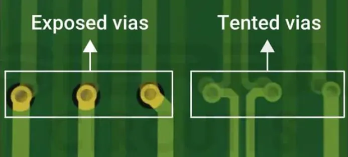
The cause was straightforward: to save board space, the design engineer placed vias directly in the BGA pads without applying resin filling and copper capping.
This is not an isolated case. From a manufacturing perspective, vias placed directly in solder pads can become a major yield risk. However, in certain applications, via-in-pad is the only technically practical solution.
The key question is not simply whether a via can be placed in a pad. The real questions are when this structure is appropriate and how it must be designed and manufactured.
Why Manufacturers Treat Unfilled Vias in Pads as a Major Risk
Risk 1: Solder Wicking Removes Solder from the Joint
Solder wicking is the root cause of many problems associated with unfilled vias in pads.
A via is essentially a small capillary tube. During reflow, the solder paste melts and the liquid solder is drawn into the via along the plated hole wall through capillary action. The process is similar to drawing liquid through a straw. As solder leaves the pad, the amount of solder available to form the joint decreases sharply. The resulting joint may become starved of solder, leading to insufficient solder, an open connection, or an intermittent connection.
One reported example illustrates the potential severity: on a 0402 component pad with an unfilled via, approximately 60% of the solder paste entered the via, reducing the solder volume on the pad by 42%. Actual results depend on the pad geometry, via structure, solder-paste properties, stencil design, and reflow profile, but the mechanism remains the same.
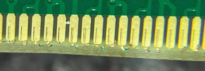
The problem does not necessarily remain on the component side of the board. Solder drawn into the via can emerge from the opposite side and form a solder ball, creating a short-circuit risk. An EMS provider may then need to perform additional manual soldering. Repeated local heating can accelerate degradation of components and pads, reducing long-term reliability.
Risk 2: Tombstoning Causes Small Components to Stand Upright
Solder wicking can also trigger a chain reaction that leads to tombstoning.
Tombstoning occurs when the two ends of a surface-mount component experience unequal soldering forces. This is especially problematic for very small packages such as 0201 and 0402 components. If one pad contains a via and the other does not, solder can be removed more quickly from the pad with the via. The resulting imbalance in solder volume and surface tension pulls one end of the component upward, leaving the component standing on end and causing an open solder joint.
Some studies have reported that an unfilled via in a component pad can increase the probability of tombstoning by as much as eight times. Smaller components are generally more vulnerable because their mass is lower and the solder surface-tension forces represent a greater proportion of the total mechanical balance during reflow.
For compact consumer-electronics products, where component miniaturization is a central design objective, this failure mode can have a serious effect on assembly yield.
Risk 3: Voids and the "Popcorn" Effect Create Hidden Reliability Problems
Even when a special via-in-pad process is selected, inadequate process control can create a less visible problem: voiding inside the solder joint.
Voids may result from several conditions:
- Incomplete resin filling leaves residual air inside the via, which can become trapped during subsequent processing.
- An uneven copper cap creates a gap between the solder paste and the copper surface.
- An unsuitable soldering temperature profile prevents volatile flux components from escaping in time.
Voids reduce the mechanical strength and thermal-conduction capability of a solder joint. The risk becomes more serious during subsequent temperature cycling. Gas trapped in a void expands and contracts as temperature changes, potentially contributing to cracking inside a BGA solder ball. The result may be an intermittent connection: the assembly passes factory testing but develops recurring failures in the field.
When Is Via-in-Pad Necessary?
Via-in-pad is not automatically unacceptable. It is a legitimate PCB design technique when the electrical, mechanical, or thermal requirements justify the additional manufacturing controls.
1. Fine-Pitch BGA Packages
When BGA pitch decreases to 0.5 mm or even 0.4 mm and below, the spacing between adjacent pads may be only about 0.2 mm. There may be no room for both a conventional via and a short escape trace between the pads.
Under these conditions, the traditional dog-bone fanout becomes impractical. The via must enter the BGA pad directly, making via-in-pad not merely an option but the only feasible routing method.

Figure 1 | Via-in-pad routing for a fine-pitch BGA package
2. Thermal Pads for Heat Dissipation
QFN and DFN packages often include a large thermal pad on the underside. Multiple thermal vias may be placed in this pad to transfer heat to an internal copper plane or to a heat-spreading structure on the opposite side of the PCB.
In this application, the vias do not normally carry the primary soldering function of an electrical pad. The center of the thermal pad does not contain an individual component terminal that must form a separate solder joint, so the solder-loss concern is different from that of a small signal or power pad.

Figure 2 | Thermal vias distributed across a QFN or DFN thermal pad
3. High-Frequency and High-Speed Signals
Placing a via directly in a pad can shorten the electrical path and reduce lead inductance. In high-speed and radio-frequency designs, every millimeter of trace length can contribute parasitic inductance, capacitance, and impedance discontinuity. At millimeter-wave frequencies, via-in-pad may provide the most favorable signal-integrity solution despite its higher fabrication cost.
This decision should still be evaluated together with the complete stackup, pad geometry, return-current path, and controlled-impedance requirements. The benefit comes from reducing the overall interconnect discontinuity, not simply from placing a via in a pad.
4. Resin Filling and Copper Capping Capability
Regardless of the application, the most important prerequisite is proper via filling and capping. For solder-bearing pads, an unfilled via should not be treated as an equivalent substitute for a filled and capped via.
A typical resin-filled and copper-capped via-in-pad process, commonly referred to as POFV, includes the following steps:
- Drilling the via.
- Plating copper in the hole.
- Filling the via with a dedicated epoxy resin.
- Curing and grinding the filled surface flat.
- Plating a copper cap over the filled via.
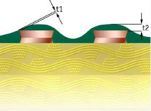
After processing, the pad surface is substantially planar and the via opening is no longer exposed. During reflow, solder paste therefore has no direct path into the hole, which greatly reduces the risk of solder wicking.
IPC-4761 Type VII is commonly associated with filled and capped via-in-pad structures. The required finish and acceptance criteria should be clearly specified in the fabrication documentation rather than left to the fabricator's interpretation.
Practical Manufacturing Recommendations
Use Conventional Fanout Whenever It Meets the Requirements
In most applications, routing a short trace out from the pad and placing the via after that trace remains the most economical and robust solution. This structure can preserve a relatively short electrical path while avoiding the additional soldering risks and fabrication cost associated with via-in-pad.
When Via-in-Pad Is Required, Define the Process Explicitly
Three basic controls should be treated as design-floor requirements:
- Control the finished via hole diameter within approximately 0.2–0.35 mm when compatible with the design. Smaller holes are generally easier to fill completely with resin, although the final value must be confirmed against the board fabricator's process capability.
- Specify IPC-4761 Type VII, or the required filled-and-capped construction, directly in the fabrication notes. Do not allow the board supplier to choose the process independently.
- Confirm that the selected PCB fabricator can produce void-free resin filling and a sufficiently flat copper cap. Not every board shop has the same capability for reliable POFV processing.
Account for the Cost
Resin filling and copper capping may increase PCB fabrication cost by approximately 30%–50%, depending on the board fabricator, layer count, and process requirements. That additional cost must be compared with the potential cost of solder defects, full-batch rework, delayed delivery, or scrapped assemblies. For a design that genuinely requires via-in-pad, the process premium can be justified by improved assembly yield and reliability.
Situations That Require Particular Caution
- 0402 and 0201 pads: The pad area is extremely small, and the via may approach or even exceed the effective pad dimensions. The resulting solder imbalance can create a severe tombstoning risk.
- Cost-sensitive consumer products: When the manufacturing budget is limited, optimize component placement and routing first. Do not adopt via-in-pad merely to simplify a layout unless the electrical or mechanical requirements demand it.
Via-in-pad is neither universally wrong nor automatically safe. An exposed via can wick solder away from the joint, promote tombstoning, and increase the risk of voids and intermittent failures. A properly filled and copper-capped via, however, can provide a necessary solution for fine-pitch BGAs, thermal pads, and demanding high-frequency interconnects.
The design decision should therefore be made jointly by the PCB designer, assembly engineer, and PCB fabricator. The most important question is not whether a via can fit inside a pad, but whether the complete design and manufacturing process can control the consequences.