An FPC that passes visual inspection and then fails electrical continuity is one of the more frustrating failures in flex design. The open is rarely a complete missing track. More often it is a partial break—hairline crack, severe undercut, or copper that has already necked down during etching—that only becomes fully open after handling, lamination pressure, or the first few bend cycles.
The root causes sit at the intersection of layout decisions and process limits. Traces drawn too narrow for the etch process, copper that cracks under flex stress, and test coverage that misses intermittent opens are the three places that keep showing up in DFM reviews.
Thin Traces and Over-Etching Leave Almost Nothing Behind
Most open-circuit failures start with a trace that was already marginal on the artwork. Designers push 50 µm or 75 µm lines because the routing density demands it. On polyimide the etch factor is higher than on FR-4. Lateral etch undercuts the resist, so a 50 µm drawn trace can finish at 30–35 µm after a normal process window. One more micron of over-etch and the copper is gone in spots.
The problem is worse at the bottom of the copper. Electrodeposited copper has a columnar grain structure; once the undercut reaches the foil interface the remaining metal lifts easily. Rolled-annealed copper holds better, but only if the etch chemistry and time are tightly controlled. Many shops still run the same etch recipe for both rigid and flex panels. That recipe is aggressive enough to clear dense rigid boards and too aggressive for fine flex lines.
When the remaining copper is that thin, any subsequent mechanical stress—coverlay lamination, punching, or even vacuum pickup—finishes the job. The open appears after manufacturing even though the design looked continuous on the Gerber.
Copper Cracks in the Bend Zone Are Usually Designed In
Static and dynamic bend areas are the second major source of FPC open circuits. Copper does not like sharp direction changes or small bend radii. A trace that runs perpendicular to the bend axis and then turns 90° right at the neutral axis creates a stress concentration. After a few cycles the copper work-hardens and a crack starts at the outer fiber.
The crack is often invisible to AOI because the coverlay is already laminated. Electrical test may still pass if the crack has not fully separated. In the field the crack propagates and the circuit opens. This is especially common when the designer places a via or a pad inside the bend region, or routes the trace with a square corner instead of a smooth arc.
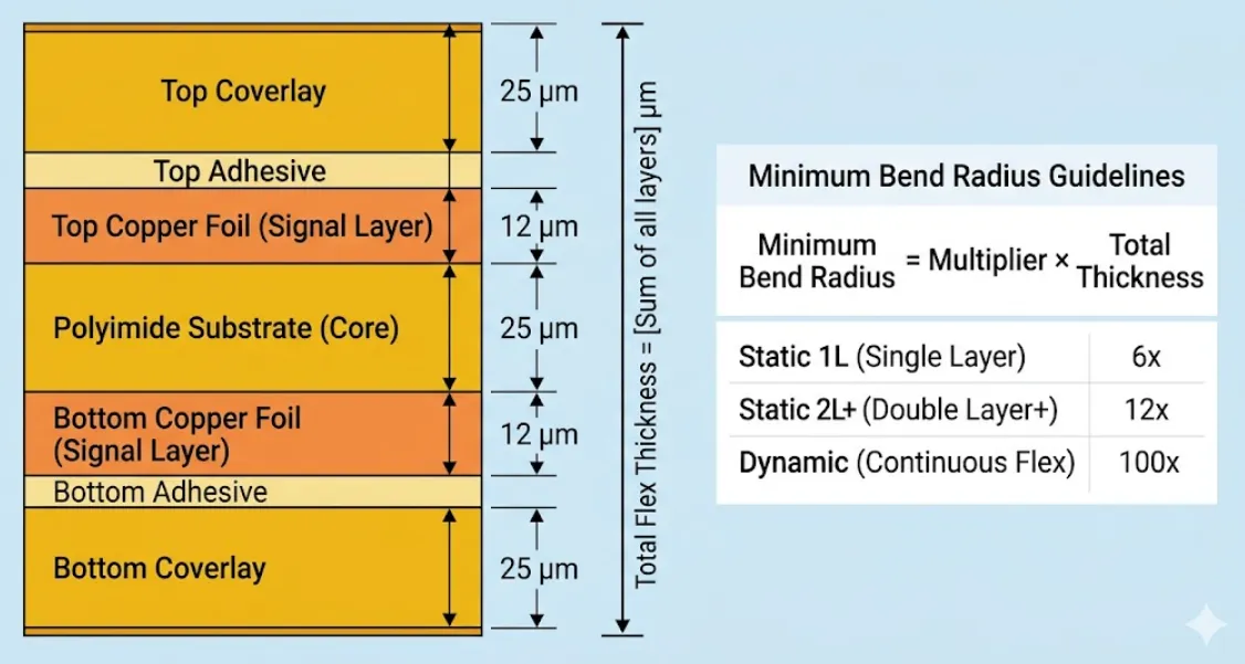
Another frequent layout choice: keeping the same copper weight across the entire flex. 1 oz copper is fine for static sections but too stiff for a dynamic hinge. The extra thickness raises the neutral-axis stress and accelerates fatigue cracking.

Why AOI Alone Does Not Catch Every Open
AOI is excellent at finding missing copper or gross shorts, but it has limits on partially cracked or undercut traces. Once coverlay is applied the optical system sees only the outline of the copper under the polyimide. A hairline crack that has not yet opened fully looks continuous. The same is true for severe neck-down: the remaining copper is still reflective enough to pass the algorithm.
Electrical test is the only reliable way to confirm continuity. Flying-probe or fixture-based testing at low current will detect a complete open. Intermittent opens caused by cracks that close under probe pressure are harder. Some shops add a light flex cycle on the tester itself before measuring, but that is not universal. High-potential testing can also expose weak points that low-current continuity misses, yet many FPC programs skip it to save time.
The practical result is that a board can leave the fab with a latent open that only appears after the customer forms the flex or after thermal cycling.
Layout and Process Changes That Actually Reduce Flexible PCB Trace Breaks
Start with the etch capability of the fabricator. If the shop’s process capability is 75 µm finished width with ±15 µm tolerance, do not draw 50 µm traces and hope for the best. Add 20–25 µm to the design width to compensate for undercut, or move to a shop that can hold tighter etch control on polyimide.
In bend regions keep traces parallel to the bend axis whenever possible. Where a turn is unavoidable, use a radius at least three times the trace width. Avoid placing pads, vias, or abrupt width changes inside the bend zone. If the copper must cross the bend, drop to ½ oz or thinner and use rolled-annealed foil. Electrodeposited copper simply does not survive repeated flex as well.
Teardrops at pad exits are cheap insurance. They reduce the stress riser where the trace meets the pad and give the etch process a little more copper to work with.
On the process side, insist on separate etch parameters for flex panels. Coverlay registration and lamination pressure also matter; excessive pressure on an already thinned trace can finish an undercut into a full open. After coverlay, a second AOI pass is useful but still secondary to a proper electrical test that includes at least one controlled bend cycle for dynamic flex parts.
Finally, treat the first-article electrical test as a design validation step, not just a production screen. If opens appear only after forming, the layout or the copper type needs revision before volume starts.
What Experience Shows Actually Works
Most FPC open circuits after manufacturing are not random process defects. They are the predictable result of drawing traces thinner than the etch process can reliably produce, routing copper through high-stress bend zones without proper geometry, and relying on optical inspection alone. The fixes are straightforward once the failure mechanism is understood: give the etch process enough copper, keep bend-region geometry gentle, and confirm continuity after mechanical stress rather than before it.
When those three points are controlled, the rate of latent flexible PCB trace breaks drops sharply.