In production we set the practical FPC laser drilling minimum hole size at 50 µm for standard UV processes. Most CAM engineers will release a 50 µm finished via on 12.5–25 µm polyimide without extra flags. Below that we go to 40 µm only after confirming material thickness, copper type, and laser station capability; 30 µm is treated as a special process that requires dedicated parameter qualification and lower daily output. CO₂ stations are almost never used for these microvias because the absorption on polyimide is poor and the heat-affected zone expands the hole unpredictably.
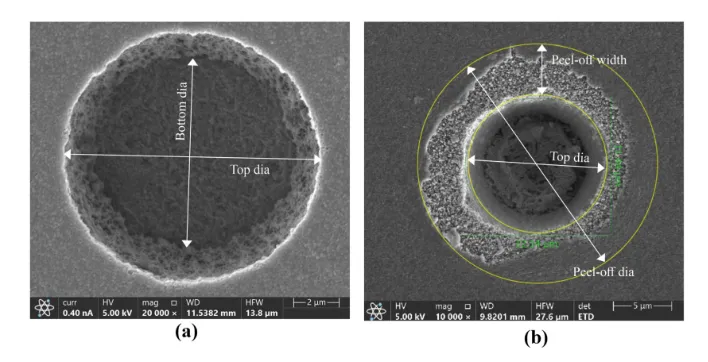
The limit shows up because the focused UV spot (355 nm) still has a practical energy density floor once you account for beam divergence, galvo positioning error, and the ablation threshold of adhesive and coverlay residues. On a typical production panel the laser must also stay registered to the etched copper pads within ±15 µm. When the programmed diameter drops below 50 µm, any small drift in focus or pulse energy leaves either an incomplete opening or a copper lip that plating cannot cover reliably.
Why UV and CO₂ stations produce different usable diameters on the same flex stack
UV laser energy is absorbed almost entirely in the top few microns of polyimide, so the ablation is clean and the wall stays nearly vertical. CO₂ energy couples poorly into pure PI and relies more on thermal decomposition; the result is a larger entrance diameter, a tapered profile, and frequent residual carbon or adhesive smear at the bottom. In practice a CO₂ station that can hold 100 µm holes on FR-4 will struggle to keep a 75 µm hole round and open on 25 µm PI. That is why every high-volume FPC line runs microvias exclusively on UV platforms when the target flex PCB microvia size is under 75 µm.
Material thickness multiplies the problem. On 12.5 µm PI the aspect ratio for a 50 µm hole is only 0.25 : 1, so the beam exits cleanly after two or three pulses. On 50 µm PI the same hole becomes 1 : 1 and residual energy at the exit side starts to undercut the bottom copper or leave a resin plug. Yield therefore falls from the mid-90 % range at 25 µm PI to the low 80 % range once the dielectric exceeds 40 µm, even if the programmed diameter stays the same.
What production sees when the diameter is pushed past the controlled limit
If a design lands on the floor with 35 µm vias and no prior process sign-off, the first symptom is incomplete ablation. AOI after laser shows a high percentage of "not open" or "partial copper remaining." Those panels either go to manual re-drill (adding cycle time) or move forward and fail electrical test after plating. Even when the hole opens, the wall roughness increases and the subsequent electroless copper coverage becomes discontinuous; that shows up later as intermittent opens after flex testing or thermal shock. Scrap rates of 15–25 % on a panel are common once the via diameter sits outside the qualified window. Shipment dates slip because the lot has to be either reworked or rebuilt with a larger via size.
Registration also suffers. The laser alignment marks themselves have a finite size; when the via is only 30–35 µm the relative contribution of any residual copper etch undercut or coverlay shift becomes large enough that a measurable fraction of vias miss the capture pad entirely. Those are pure scrap.
How the factory keeps 50 µm and occasional 40 µm vias under control
CAM first measures the actual dielectric thickness after lamination and sets the laser recipe accordingly. For a 50 µm target we typically program 45–48 µm to allow for a small amount of wall taper and still finish at 50 µm after plating. Pulse energy, frequency and number of passes are locked to the specific PI type and copper weight; a change in supplier or adhesive system forces a new parameter set. The beam is focused to the top copper surface and the Z-height is verified every panel lot. Alignment is done to etched fiducials, never to the tooling holes, because the copper-to-laser registration is the critical one.
On the design side we enforce a minimum pad diameter of 150 µm for a 50 µm via (giving ≥50 µm annular ring after all tolerances). Coverlay openings are held at least 100 µm larger than the via so that laser debris does not get trapped under the coverlay edge. If the stack includes adhesive, we add a short pre-ablation or plasma clean step to remove residual organics before plating. These steps are written into the process traveler and checked at first-article inspection.

For the occasional 40 µm request we move the job to a dedicated high-precision UV station with tighter galvo calibration and slower table speed. Panel size is often reduced so that beam walk remains under 10 µm across the usable area. Yield is accepted at 85–90 % and the customer is quoted the corresponding cost adder. Anything smaller than 40 µm is treated as a development lot only; production capacity is not committed until a full DOE confirms stable opening rate and plating quality.
When the factory will relax the 50 µm floor
Prototype or engineering lots of fewer than 20 panels can run 35–40 µm vias provided the customer accepts the risk of lower yield and longer cycle time. Designs that use only one or two critical microvias per circuit, rather than dense arrays, also get more latitude because a single failed via does not scrap the entire panel. Thick-copper or multi-layer flex constructions almost never receive exceptions; the combination of higher aspect ratio and thermal mass makes the process window too narrow. In every case the relaxation is documented on the traveler and the first-article report so that the next volume order returns to the standard 50 µm rule.
The controlling factor remains the same: keep the finished flex PCB microvia size inside the qualified laser and material window, or accept the yield and schedule consequences that follow when it is not.