Most FPC short circuit failures between adjacent traces are not random. They come from three predictable sources: finished spacing that ends up tighter than the process can hold, residual copper left after etching, or conductive foreign material that bridges the gap later. When a flexible PCB trace short shows up in electrical test or field returns, these are the first places to look.
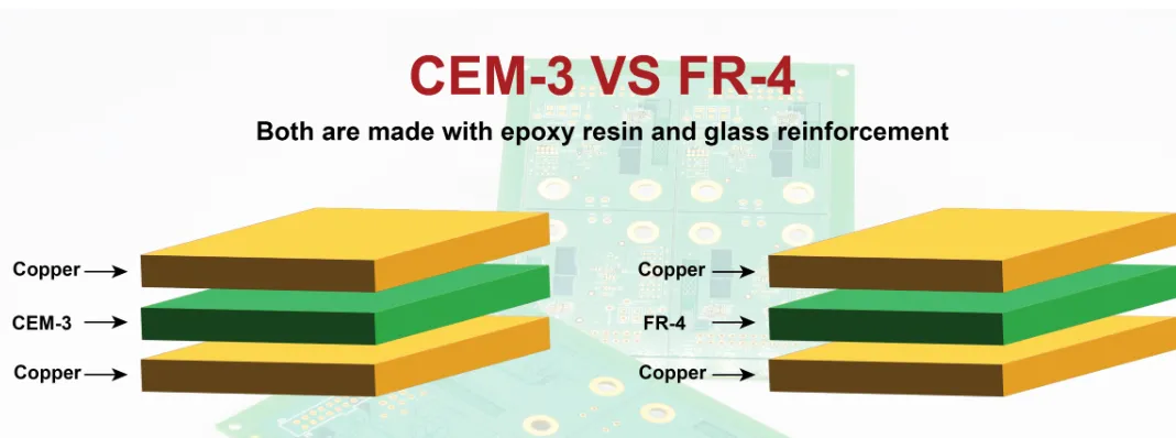
The root decision is almost always made at layout. Designers treat polyimide the same way they treat FR-4 and apply rigid-board clearances. That works until the etch chemistry and the thin copper start interacting differently.
Why Trace Spacing That Looks Safe on the Screen Becomes a Short After Etch
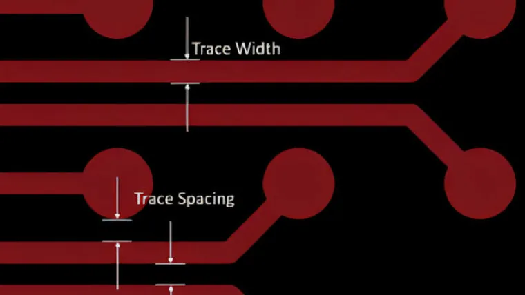
Flexible copper is typically 12 µm or 18 µm. The etch undercut on polyimide is proportionally larger than on thicker rigid copper. A 75 µm designed gap can finish at 45–55 µm once the lateral etch is finished. At that point the process window is gone.
Any local variation in spray pressure, bath temperature, or copper grain structure reduces the gap further. In dense areas the etchant also has more difficulty circulating, so the undercut becomes non-uniform. One side of a pair of traces can be over-etched while the other still has residual copper hanging into the space.
That is the classic flexible PCB trace short that only appears after coverlay is applied or after the board has been flexed a few times. The residual bridge is thin enough that AOI sometimes misses it, yet thick enough to create a hard short under mechanical stress.
Residual Copper and Foreign Material: The Two Other Frequent Culprits
Incomplete etching is especially common near large copper pours or in regions where the designer left isolated copper features. The etchant depletes locally and leaves microscopic copper islands or "whiskers" that later contact the neighboring trace when the flex is bent.
Foreign material is less elegant but equally common. Metal particles from punching dies, copper dust from routing, or even conductive adhesive residue from coverlay lamination can land between traces. On rigid boards these particles often get washed off or are large enough to be caught. On FPC the surface is softer and the gaps are smaller, so the particle can embed and stay.
Once coverlay is laminated the particle is trapped. Electrical test may still pass if the contact pressure is low, but the first mechanical cycle or humidity exposure turns it into a permanent short.
How High-Density Layouts Collapse the Process Window
When line/space moves below 50/50 µm the numbers stop being forgiving. Etch factor becomes critical. A typical alkaline etch on 12 µm copper already produces roughly 1:1 undercut. Any additional 10 µm of lateral etch removes 20 % of the designed spacing.
Registration between the artwork and the copper also tightens. LDI helps, but not every fabricator runs LDI on every layer. Traditional film still has dimensional instability that can shift a 40 µm gap by 15 µm across a panel.
At these densities the probability of an FPC short circuit rises sharply because the same absolute process variation that was acceptable at 100 µm spacing now consumes half the clearance. Designers who push 40/40 µm without confirming the fabricator's actual capability data are essentially designing to the edge of the process.
What Etching Control and AOI Actually Catch—and What They Miss
Good fabricators control etch with continuous monitoring of copper thickness, bath chemistry, and spray uniformity. They also run coupon etch-rate tests on every lot. Even then, local residual copper in dense pockets can escape visual inspection.
AOI after etch is the primary defense. Modern systems detect most hard bridges and large residual copper. They are less reliable on very thin filaments or on boards that have already been partially covered by coverlay. Flex warpage also reduces AOI resolution compared with rigid panels.
Electrical test after coverlay catches the remaining hard shorts, but it does not catch latent bridges that only close under bending or thermal cycling. Those show up later as intermittent field failures.
The practical takeaway is simple: process controls reduce the rate, they do not eliminate the root cause. The root cause is still the designed spacing versus the real process capability.
Layout Rules That Actually Prevent Flexible PCB Trace Shorts
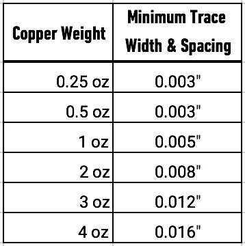
Start with the fabricator's published capability table for the specific copper weight and polyimide type, not with a generic IPC number. For standard 12 µm copper on polyimide, many reliable shops still prefer 75 µm finished minimum spacing for production volumes. Tighter is possible with LDI and controlled etch, but only when the design is reviewed against their actual process data.
Account for etch factor explicitly. If the fabricator states a 1:1 etch factor on 18 µm copper, a 60 µm designed gap will finish near 42 µm. Design the artwork so the finished gap stays inside the process window after undercut.
Avoid isolated copper features that create local etchant starvation. If copper balancing is required, use a consistent hatch rather than solid pours next to fine traces.
Keep coverlay openings and adhesive squeeze-out in mind. Adhesive that flows into a tight gap can either create a conductive path if contaminated or mechanically stress a residual copper filament until it fails.
Finally, add a small amount of extra clearance in high-flex zones. The mechanical strain of repeated bending can close a marginal gap that would have survived on a static rigid board.
When these rules are followed, the incidence of FPC short circuit between traces drops dramatically. Most remaining failures then shift to handling or assembly damage rather than layout-induced process violations. That is the difference between designing to the artwork and designing to the finished part that actually comes off the production line.