High Density Interconnect PCB for AI Hardware: Designing Reliable Humanoid Robot Electronics
The development of humanoid robots and advanced mobile manipulators is driven by the need for machines that can operate effectively in human-centric environments. These systems combine bipedal mobility, dexterous manipulation, real-time perception, and embodied intelligence, placing extreme demands on the underlying printed circuit boards (PCBs). From high-speed sensor fusion and AI inference to precise motor control and power management, the performance, reliability, and safety of humanoid robots depend heavily on sophisticated PCB engineering.
As AI compute density increases, high density interconnect PCB for AI hardware becomes increasingly important for integrating processors, memory, high-speed interfaces, sensor processing, and power delivery within constrained robotic platforms. HDI structures provide additional routing capacity through microvias, blind vias, fine-line features, and optimized multilayer stack-ups, helping engineers accommodate increasingly complex AI electronics without proportionally increasing PCB size.
At Aivon, we develop and manufacture high-reliability PCBs that serve as the backbone of next-generation robotic platforms, supporting the transition from traditional industrial automation to intelligent, adaptive humanoid systems.

Why High Density Interconnect PCB for AI Hardware Matters in Humanoid Robots
Humanoid robots are built in human-like forms to leverage existing infrastructure such as stairs, tools, vehicles, and workspaces without requiring costly environmental modifications. This anthropomorphic design enables broader deployment in healthcare, elder care, logistics, manufacturing, and domestic assistance.
The physical constraints of humanoid platforms create demanding PCB requirements. Electronics must fit inside limbs, joints, torsos, and compact computing compartments while maintaining sufficient electrical and mechanical performance.
PCB design must address several key challenges:
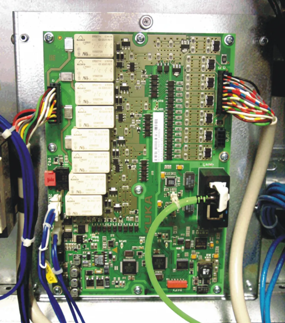
- Compact, lightweight, and distributed electronics: Humanoids require numerous distributed control boards, often positioned near individual limbs or joints, together with one or more central compute units. This favors HDI PCBs with microvias, blind and buried vias, fine-line routing, and thin laminates to reduce board size while maintaining interconnection density.
- High-density AI hardware: AI processors, GPUs, NPUs, and memory devices can use high-pin-count BGA packages and high-speed interfaces. HDI structures help provide the escape routing and layer-to-layer transitions required by these dense footprints.
- Dynamic mechanical stress: Constant motion, vibration, and potential impacts demand rigid-flex or flexible-rigid PCB structures, suitable high-Tg materials, controlled CTE characteristics, and robust solder joints.
- Real-time coordination: Synchronized control of many degrees of freedom requires low-latency, high-bandwidth communication buses such as EtherCAT, TSN, or high-speed SerDes. These interfaces require controlled impedance, appropriate return paths, and accurate length matching.
- Power and thermal density: Compact AI computing and high-torque actuators can create concentrated power loads. PCB stack-ups must therefore support efficient power delivery, current distribution, and thermal dissipation.
For these reasons, the role of a high density interconnect PCB for AI hardware extends beyond simple miniaturization. The PCB becomes part of the system architecture that connects compute, sensing, communication, motion control, and power functions.

AI Robot HDI PCB Design for Edge Computing and Embodied Intelligence
Embodied intelligence integrates perception, cognition, and action in physical bodies, allowing robots to learn and adapt through interaction with the real world. Mobile manipulators, including wheeled or legged platforms with robotic arms, represent a practical step toward full humanoid systems by combining mobility with dexterous task execution.
AI computing requirements place particularly strong demands on the PCB.
Critical PCB requirements for embodied AI include:
- High-performance AI acceleration: Running large vision-language-action models on the edge requires PCBs capable of supporting powerful SoCs, GPUs, or NPUs with high-speed DDR/LPDDR interfaces, PCIe Gen4/5 lanes, and optimized power delivery networks.
- High-density processor and memory routing: AI processors and memory devices often use dense BGA packages. An AI robot HDI PCB can use microvias, via-in-pad structures, and additional routing layers to support compact BGA escape routing and short interconnections.
- Multi-modal sensor fusion: Cameras, LiDAR, IMUs, force-torque sensors, and tactile arrays require clean analog front ends, isolated power domains, and high-speed digital interfaces. Layout separation between analog, digital, and power sections helps reduce noise and crosstalk.
- Real-time control loops: Low-latency motor drivers and joint controllers require dedicated motion-control PCBs or close integration with the main compute architecture. High-current traces, thermal vias, and robust grounding become important in these regions.
- High-speed data movement: PCIe, SerDes, memory interfaces, and camera links require controlled impedance, short signal paths, appropriate via structures, and careful reference-plane management.
For compact AI robots, HDI technology can reduce routing congestion around high-pin-count processors while helping engineers integrate compute and sensor interfaces into constrained mechanical spaces. The actual HDI structure should be selected according to package pitch, layer count, dielectric thickness, via capability, signal-speed requirements, and manufacturing process capability.
AI Server Motherboard High Density PCB: What Humanoid AI Hardware Can Learn from Data-Centric Computing
AI server motherboards and humanoid robot compute boards share several PCB-level challenges, including high compute density, high-speed memory interfaces, high-speed serial links, complex power delivery networks, and concentrated thermal loads.
An AI server motherboard high density PCB must provide reliable electrical connections between processors, memory, accelerators, storage interfaces, and power systems. Humanoid AI hardware faces many of the same signal-integrity and power-integrity challenges, but adds stricter constraints on size, weight, vibration, and distributed system architecture.
Several PCB design principles can therefore be relevant to both platforms:
- High-density BGA escape routing: Dense processor packages require carefully planned fan-out and layer transitions.
- Controlled impedance: High-speed interfaces need consistent impedance through traces, vias, connectors, and transitions.
- Power delivery optimization: AI processors can create substantial transient current demand, requiring carefully designed power planes and decoupling networks.
- Thermal management: Compute-intensive devices require low-resistance thermal paths and sufficient copper area.
- Short high-speed interconnects: Reducing unnecessary routing distance can help control insertion loss, reflections, and timing margins.
However, humanoid robots cannot simply adopt a server PCB architecture without modification. Their electronics must accommodate distributed joint controllers, sensor modules, mechanical movement, battery operation, and strict mass constraints. HDI and rigid-flex technologies can help translate high-density computing concepts into a more compact and mobile hardware architecture.

AI Robot PCB Reliability: Signal Integrity, Power, Thermal, and EMI Challenges
Humanoid robots generate significant engineering constraints at the PCB level. Reliability must be considered together with electrical performance, mechanical movement, and thermal behavior.
Signal Integrity: High-speed interfaces between cameras, IMUs, processors, memory, and communication modules must maintain signal quality despite compact routing and electromagnetic interference from motors. Controlled impedance routing, differential-pair tuning, appropriate via structures, back-drilled vias where applicable, and low-loss laminates can help manage these requirements.
For HDI designs, microvia transitions and via-in-pad structures should be evaluated as part of the complete high-speed channel. Changes in reference planes, unnecessary stubs, and poorly controlled layer transitions can affect high-speed performance.
Power Distribution and Efficiency: Battery-powered operation combined with multiple high-torque actuators requires sophisticated power management. Heavy copper layers, multi-phase voltage regulators, optimized power planes, and distributed decoupling can help minimize voltage droop and resistive losses.
Power architecture must also account for the relationship between central AI computing and distributed motor-control electronics. Separating noisy high-current paths from sensitive sensor and communication circuits can reduce unwanted coupling.
Thermal Management: Dense compute clusters and motor drivers produce concentrated heat in compact spaces. Solutions include thick copper planes, thermal-via arrays, large copper spreading areas, and high-Tg materials. In selected high-power regions, metal-core or other thermally optimized substrate structures may also be considered according to the mechanical and electrical requirements.
EMI/EMC and Reliability: Motor drivers and high-frequency switching circuits create challenging electromagnetic environments. Proper grounding, shielding, return-path control, component placement, and multilayer stack-up design are essential for preventing interference with sensitive sensors and wireless communication modules.
These factors directly influence AI robot PCB reliability. Electrical testing alone is not sufficient; the PCB must also be evaluated under representative thermal, mechanical, and operational conditions.
HDI PCB Technologies for AI Robots, Sensor Modules, and High-Density Computing
Several PCB technologies can support the growing hardware requirements of humanoid robots and mobile AI systems.
HDI and Rigid-Flex Designs
HDI structures enable compact routing through microvias, blind vias, fine-line features, and multilayer interconnections. Rigid-flex structures can additionally allow boards to fold into humanoid limbs, joints, or torso assemblies.
The combination can reduce cable length and connector requirements while providing more freedom for mechanical integration.
High-Speed Multilayer Stack-Ups
AI hardware requires high data throughput from vision systems, processors, memory, and inter-board communication. Multilayer stack-ups can provide dedicated power and ground planes while supporting controlled-impedance signal layers.
Stack-up design should consider dielectric thickness, copper distribution, reference-plane continuity, via structures, and the requirements of the specific high-speed interfaces.
AI Robot Sensor Module PCB Design
An AI robot sensor module PCB may integrate cameras, IMUs, LiDAR interfaces, force-torque sensors, tactile sensing electronics, and local processing circuits within a highly constrained mechanical area.
HDI structures can help route dense sensor interfaces while maintaining compact dimensions. Analog and digital sections should be carefully separated, with appropriate grounding and power filtering to protect sensitive sensor signals from motor and switching noise.
Automotive and Industrial-Grade Materials
High-Tg FR-4, low-CTE laminates, and halogen-free materials can be selected according to the expected thermal, mechanical, and environmental conditions. Material selection should consider temperature cycling, vibration, dimensional stability, dielectric performance, and manufacturing compatibility.
Integrated Power and Motion Control
Custom boards combining MCUs, motor drivers, current sensing, feedback interfaces, and communication circuits can reduce cabling and improve system responsiveness. In distributed architectures, local control boards can be positioned close to actuators while communicating with central compute units.
Secure and Upgradable Architectures
AI robots may require secure boot, OTA updates, hardware security modules, and protected communication interfaces. PCB architecture should provide suitable support for these electronic security functions while maintaining serviceability and upgrade flexibility.
Together, these technologies help bridge the gap between current mobile manipulators and future humanoid platforms capable of increasingly complex adaptive behaviors.
AI Robot PCB Prototype and Manufacturing Considerations
Producing PCBs for humanoid robots requires close collaboration between design and fabrication teams. This becomes particularly important when an AI robot PCB prototype contains HDI structures, high-speed interfaces, fine-pitch components, and rigid-flex sections.
Key manufacturing considerations include:
- DFM review: Evaluate microvia dimensions, via-in-pad structures, BGA escape routing, registration, copper balance, and stack-up before fabrication.
- Controlled impedance: Verify trace geometry, dielectric thickness, copper thickness, and stack-up construction for high-speed interfaces.
- Registration control: Dense HDI structures require appropriate layer-to-layer registration throughout sequential buildup.
- Microvia reliability: Microvia geometry, copper plating, filling, and interfaces should be evaluated according to the actual HDI construction.
- Mechanical reliability: Connector regions, mounting points, rigid-flex transitions, and high-vibration areas require appropriate structural design.
- Comprehensive testing: Thermal, mechanical, electrical, and functional testing should reflect the intended robotic operating environment.
- Prototype-to-production scalability: The prototype process should identify manufacturing constraints early so that the final design can transition to repeatable volume production.
Prototype development is particularly useful for validating the interaction between PCB architecture and the robot's mechanical structure. An early prototype can reveal issues involving thermal concentration, connector loading, cable routing, vibration, and electromagnetic interference before larger production volumes are introduced.
AI Robot Power PCB and High-Density Hardware Development Trends
As humanoid robots become more capable, PCB requirements will increasingly be shaped by the combination of AI computing and distributed electromechanical systems.
AI processors are likely to demand greater compute density and more efficient power delivery, while motors and actuators require localized high-current control. This creates a need for AI robot power PCB architectures that balance current capacity, thermal performance, electromagnetic compatibility, and physical size.
Future robotic platforms may also use more distributed computing, placing dedicated processing and control functions closer to sensors and actuators. This can reduce communication latency but increases the number of compact PCB assemblies throughout the robot.
At the same time, higher compute density will continue to increase thermal challenges. PCB designers may need to coordinate HDI stack-up design, power distribution, thermal spreading, material selection, and mechanical integration as a single system-level problem.
The future of humanoid robotics therefore depends not only on more capable processors and sensors, but also on PCB architectures that can reliably connect and power these technologies within a moving, weight-constrained platform.
Aivon supports robotics developers and manufacturers with PCB solutions ranging from stack-up design and DFM feedback to complex multilayer, HDI, and rigid-flex production. These capabilities help translate advanced humanoid and mobile manipulator concepts into reliable electronic assemblies suitable for demanding robotic environments.
Ready to bring your humanoid robot or embodied AI platform to life? Contact the Aivon team for guidance on PCB design, material selection, HDI stack-up development, and manufacturing strategies tailored to advanced robotics.
FAQ
Q1: Why Is HDI Important for AI Robot PCBs?
A1: HDI is important for AI robot PCBs because AI processors, memory devices, sensors, and high-speed interfaces require high routing density within compact mechanical spaces. Microvias, blind vias, fine-line routing, and multilayer structures can provide additional interconnection capacity without significantly increasing board size. HDI must still be matched to package pitch, signal-speed requirements, material selection, and the manufacturer's actual fabrication capabilities.
Q2: What Is an AI Robot HDI PCB?
A2: An AI robot HDI PCB is a high-density printed circuit board designed to support computing, sensing, communication, or control functions in an AI-enabled robotic platform. It may integrate processors, memory, sensor interfaces, motor-control circuits, and high-speed communication links. Microvias and fine-line routing can help accommodate dense components while maintaining the compact form factors required by humanoid and mobile robots.
Q3: What Makes an AI Robot Sensor Module PCB Different?
A3: An AI robot sensor module PCB must often accommodate multiple sensing technologies within a small mechanical area. Cameras, IMUs, LiDAR interfaces, force sensors, and tactile arrays can require different electrical characteristics and noise-control strategies. The PCB therefore needs careful analog and digital separation, appropriate power filtering, controlled high-speed routing, and mechanical integration suitable for continuous robotic movement and vibration.
Q4: How Can Engineers Improve AI Robot PCB Reliability?
A4: AI robot PCB reliability depends on electrical, thermal, mechanical, and manufacturing controls working together. Engineers should evaluate signal integrity, power delivery, thermal paths, solder-joint strength, vibration resistance, connector interfaces, and HDI microvia structures. Prototype testing can help identify weaknesses before production. Reliability validation should reflect the actual temperature, vibration, mechanical movement, and operating conditions expected during robotic operation.
Q5: What Should Be Considered When Developing an AI Robot PCB Prototype?
A5: An AI robot PCB prototype should validate both the electrical design and its integration into the robot. Engineers should review HDI stack-up, BGA escape routing, impedance control, thermal behavior, power delivery, sensor interfaces, connector placement, and mechanical clearances. Prototype testing should also consider vibration, temperature cycling, EMI, and functional performance so that design issues can be addressed before volume manufacturing.
Q6: What Is the Role of an AI Robot Power PCB?
A6: An AI robot power PCB distributes and regulates electrical power for processors, sensors, communication electronics, and high-current actuators. It may incorporate voltage regulators, power planes, current sensing, thermal vias, and protection circuits. The design must balance current capacity, efficiency, heat dissipation, EMI control, and physical size. In distributed robots, multiple localized power boards may work together with a central power architecture.