PCB PDN
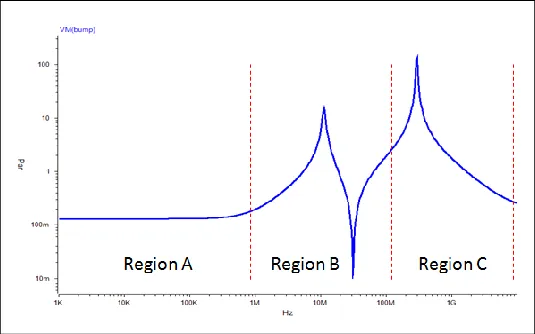
The PCB PDN, or Power Distribution Network in printed circuit boards, plays a critical role in ensuring reliable power delivery to electronic components. This tag encompasses a range of topics focused on designing, analyzing, and optimizing PDNs to maintain power integrity, minimize voltage fluctuations, and reduce electromagnetic interference in modern electronics. For engineers and designers searching for PCB PDN resources, understanding these elements is essential to prevent common issues such as signal degradation, thermal hotspots, or system failures in high-speed circuits. In practice, effective PCB PDN design involves strategic layer stacking, via placement, and decoupling capacitor selection to achieve low impedance paths across frequency ranges. Professionals often rely on simulation tools like SPICE or dedicated PDN analyzers to model impedance profiles and identify resonances before fabrication. Best practices include incorporating plane capacitance, using power integrity checks during layout, and adhering to guidelines for current return paths to enhance overall board performance. These approaches are particularly valuable in applications like consumer electronics, automotive systems, and data centers, where power efficiency directly impacts reliability and cost. Readers interested in deepening their knowledge will find articles here that offer step-by-step tutorials on PDN simulation, case studies from real-world projects, and troubleshooting tips for common design challenges. By applying these insights, you can refine your PCB designs to meet stringent specifications and improve product longevity.
Technical Articles