Coupons
Help
  • FAQ
    browse most common questions
  • Live Chat
    talk with our online service
  • Email
    contact your dedicated sales:

Engineering Cases

Engineering Cases focuses on real PCB engineering reviews, manufacturing challenges, and production optimization processes from actual fabrication projects. This category highlights how different PCB designs are evaluated and adjusted during engineering review, covering topics such as stack-up analysis, impedance control, drill optimization, copper balancing, solder mask alignment, DFM review, and production risk assessment across various PCB applications. The content in this section is based on practical manufacturing scenarios rather than theoretical introductions. Each engineering case demonstrates how specific PCB issues are identified, analyzed, and resolved during production preparation and fabrication. These records help engineers, purchasers, and hardware teams better understand the relationship between PCB design decisions and manufacturing stability, yield control, and process reliability. Topics may include multilayer PCB engineering review, HDI process optimization, flexible PCB manufacturing considerations, heavy copper processing adjustments, surface finish selection, Gerber data verification, and other real-world PCB production experiences. By organizing engineering challenges and process solutions into structured case content, this category provides valuable insight into practical PCB manufacturing and engineering workflow management.

 
How PCB Manufacturers Improve Solder Mask Yield in HDI Production
PCB Manufacturing Defects Design For Manufacturing (DFM) HDI PCB PCB Reliability Cost Optimization Solder Mask Adhesion Microvia Manufacturing Solder Mask Expansion

How PCB Manufacturers Improve Solder Mask Yield in HDI Production

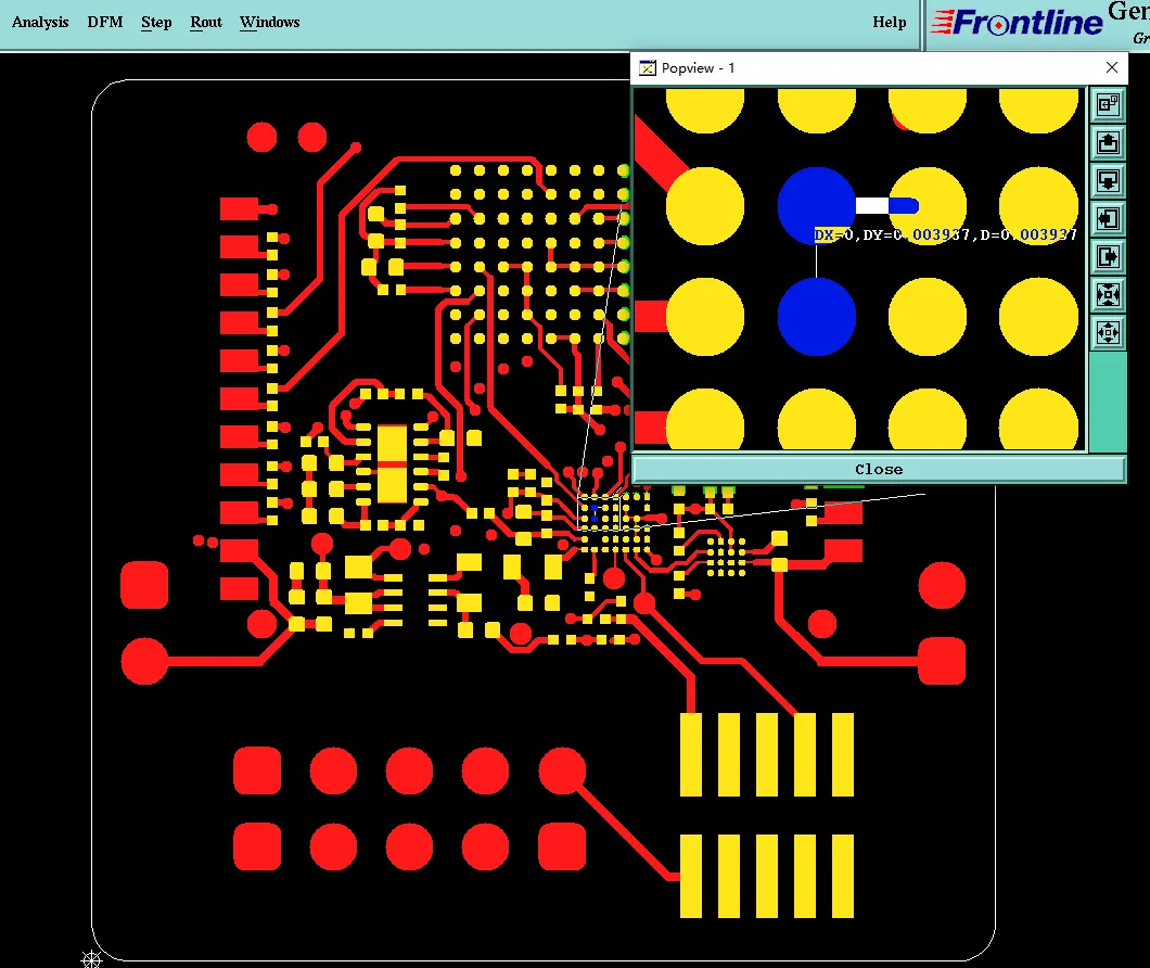
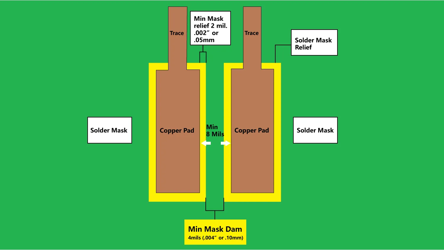
Discover how PCB manufacturers enhance HDI solder mask process yield through precise solder mask exposure settings, accurate window opening compensation, and strict bridge width control. Learn real factory CAM adjustments, registration handling, and production strategies that reduce defects and boost first-pass yields on high-density interconnect boards.

DFM Fixes for Non-Plated Slots, Gold Fingers & Trace Extensions in 4-Layer FR4 PCB
PCB Manufacturing Defects PCB Panelization Design For Manufacturing PCB Trace Routing Rigid PCB Gold Plating PCB Edge Plating

DFM Fixes for Non-Plated Slots, Gold Fingers & Trace Extensions in 4-Layer FR4 PCB

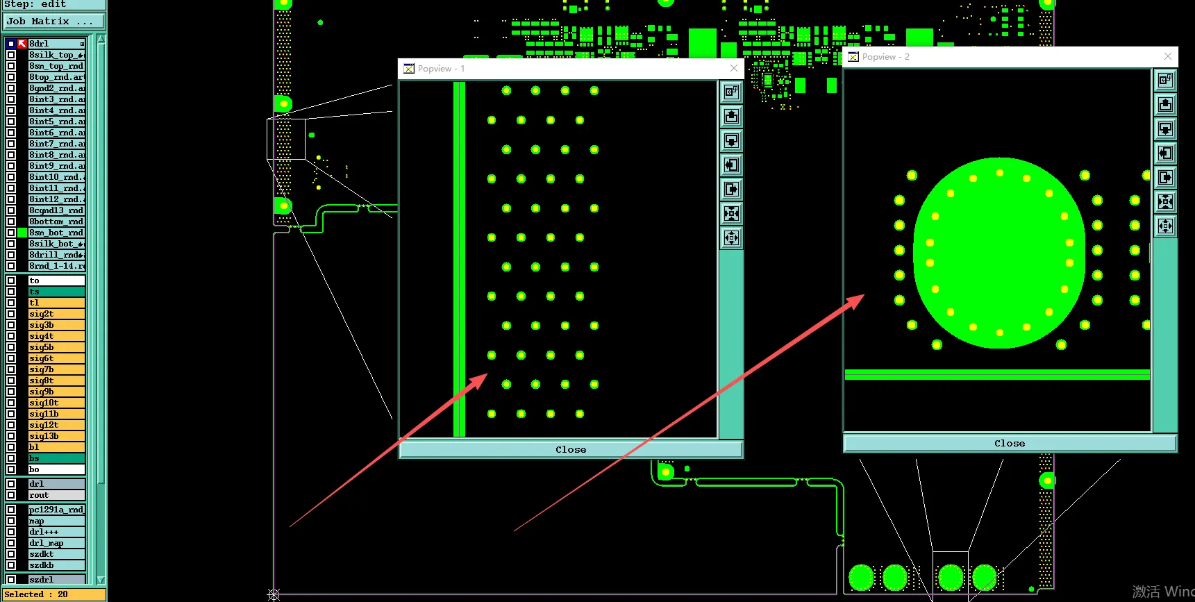
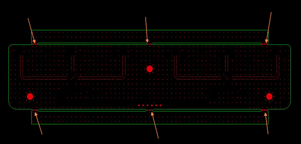
Real CAM engineering case on a 4-layer FR4 PCB where non-plated 0.5mm slots, external trace extensions, gold finger bevels, and panelization spacing required EQ clarification. Learn practical DFM adjustments that prevented routing defects, edge copper exposure, and assembly issues for reliable production.

How DFM Review Prevented Silkscreen and Tolerance Issues in 4-Layer FR4
FR4 PCB PCB Stackup Silkscreen Rigid PCB Silkscreen Legibility High Volume PCB

How DFM Review Prevented Silkscreen and Tolerance Issues in 4-Layer FR4

In this 3000-piece 4-layer FR4 order, DFM analysis identified risks including insufficient silkscreen character height, slot hole tolerance requirements, and stackup alignment. Learn how proactive engineering confirmations and adjustments ensured clear markings, reliable dimensions, and successful high-volume production while avoiding legibility failures and process deviations.

DFM Review Prevented Stiffener and Hole Risks in Thin Flex PCB
PCB Materials PCB Reliability Design For Manufacturing EMI Shielding Flex PCB Materials Flexible Polyimide PCBs PCB Stackup Design Ultra Thin PCB

DFM Review Prevented Stiffener and Hole Risks in Thin Flex PCB

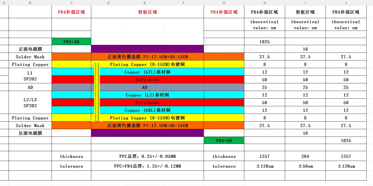
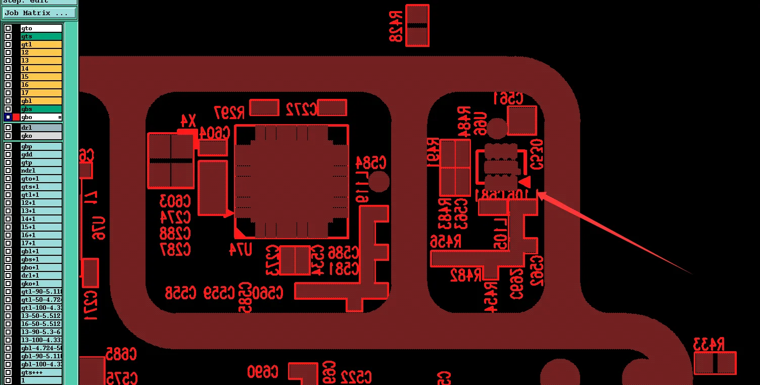
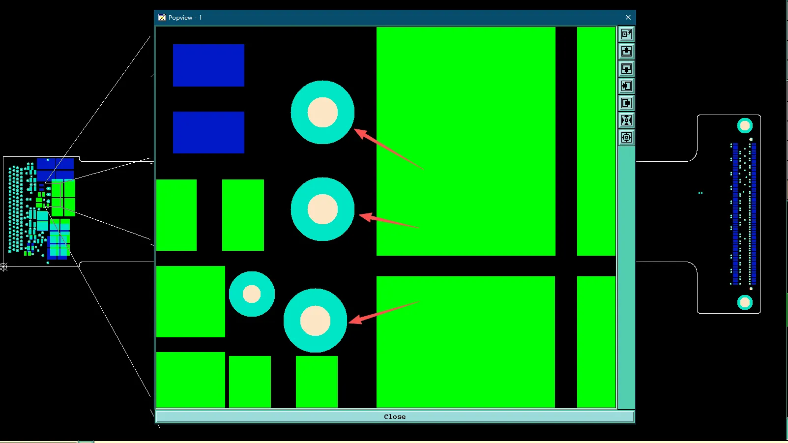
For this ultra-thin 3-layer flex PCB with FR4 stiffener and EMI shielding, DFM analysis uncovered critical issues including stiffener overhang covering holes, PTH/NPTH definition mismatches, and material feasibility for 0.15mm thickness. Discover how preventive engineering adjustments ensured proper alignment, correct plating, and successful production, helping avoid assembly failures and reliability problems in flexible circuit designs.

How Panelization Conflict Delayed Single Piece Delivery in 1-Layer PCB
PCB Fabrication Design For Manufacturing Gerber Files PCB Tolerances PCB Design Review PCB Panel Optimization PCB Routing Strategies

How Panelization Conflict Delayed Single Piece Delivery in 1-Layer PCB

Learn how mismatched panelization data and process edge requirements triggered an Engineering Question for a 1-layer FR4 PCB order. This CAM review case examines the investigation into V-CUT incompatibility, hole attributes, Gerber layer discrepancies, resolution through routing confirmation, and key lessons for designers to align data files with single piece delivery expectations for smooth manufacturing.

Resolving 12 layer FR4 PCB Copper Thickness and Impedance Conflicts
Signal Integrity Design For Manufacturing (DFM) PCB Copper Weight PCB Impedance High-Layer PCB Impedance Mismatch PCB Design Review PCB Stackup Design

Resolving 12 layer FR4 PCB Copper Thickness and Impedance Conflicts

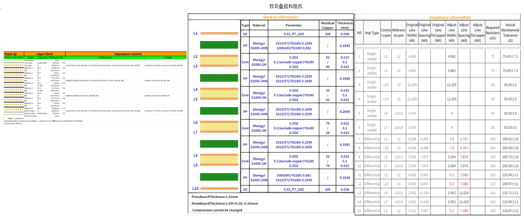
Explore how conflicting copper thickness specifications across stackup and impedance documents triggered a key Engineering Question during CAM review of a 12-layer FR4 PCB. This engineering case details the investigation into file format conflicts, via mask alignment, proposed stackup adjustments for impedance control, resolution process, and practical lessons for designers to ensure consistent documentation and manufacturable multilayer boards.

How DFM Review Secured Impedance Control in 6-Layer FR4 PCB
Design For Manufacturing (DFM) High-Speed PCB PCB Reliability Solder Mask Application Signal Reflections PCB Copper Pour PCB Stackup Design

How DFM Review Secured Impedance Control in 6-Layer FR4 PCB

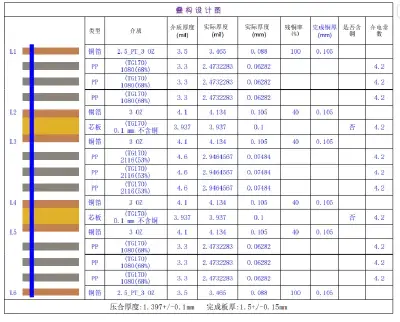
In this 6-layer FR4 project, DFM analysis identified critical risks including non-standard stackup, marginal trace widths for 90 ohm impedance, missing copper pour on L4 for 50 ohm control, and absent solder mask openings. Learn how proactive engineering adjustments ensured accurate impedance, reliable plating, and successful production, helping designers avoid common signal integrity and manufacturability issues.

Why Impedance Line Mismatches Triggered EQ in Multi-Layer PCB Production
PCB Manufacturing Defects Signal Integrity PCB Impedance Multilayer PCB Design For Manufacturing Impedance Discontinuity PCB Stackup Design DFM For PCB

Why Impedance Line Mismatches Triggered EQ in Multi-Layer PCB Production

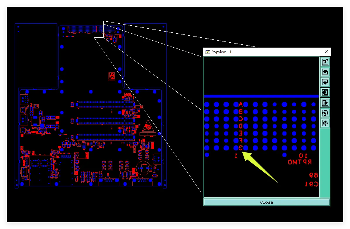
Discover how inconsistent impedance line identification between customer tables and production files triggered a critical Engineering Question during CAM review of a 8-layer FR4 PCB. This case details the engineering investigation, supporting mechanical concerns like stamp holes and silkscreen clearance, resolution process, and key lessons for designers to prevent similar data conflicts and ensure manufacturable impedance control.

Critical PCB DFM Review for Small Volume FR4 Production Runs
PCB Panelization Design For Reliability (DFR) Solder Mask PCB Reliability Stencil Aperture High Volume PCB PCB Design For Manufacturing

Critical PCB DFM Review for Small Volume FR4 Production Runs

In a 5400-piece 2-layer FR4 order, DFM analysis uncovered tight stamp hole spacing, missing solder mask openings on pads, and challenging square slots that threatened panel integrity and yield. Learn how preventive engineering clarifications avoided breakage, ink coverage issues, and assembly failures, ensuring reliable high-volume production and long-term board quality.

How DFM Review Prevented Via Reliability Risks in a 2-Layer FR4 PCB
PCB Manufacturing Defects Solder Mask PCB Reliability Solder Joint Reliability Design For Manufacturing Via Failure Modes Rigid PCB

How DFM Review Prevented Via Reliability Risks in a 2-Layer FR4 PCB

Discover how our DFM analysis identified critical via solder mask issues, plated slot conflicts, and dimensional discrepancies in a 2-layer FR4 working file. We explains the preventive actions taken to avoid ink intrusion, solder bead entrapment, and yield loss—ensuring reliable production and long-term PCB performance. Learn key lessons for better manufacturability.


2026 AIVON.COM All Rights Reserved
Intellectual Property Rights | Terms of Service | Privacy Policy | Refund Policy