The Ten Most Common Beginner Mistakes in PCB Layout
Default DRC, right-angle traces, distant decoupling, split planes, thin power traces, and missing test points still cause most first-board failures. Check these ten items.
Printed Circuit Board (PCB) design forms the backbone of modern electronics, enabling the creation of compact, efficient, and reliable devices that power everything from smartphones to industrial machinery. In this category, readers gain access to a comprehensive collection of resources dedicated to mastering PCB design principles and techniques. Whether you are a seasoned engineer refining complex layouts or a newcomer learning the fundamentals, these articles provide the knowledge needed to tackle real-world challenges in electronics development. The scope of PCB design covered here extends from initial schematic capture to final board fabrication and testing. Articles delve into essential topics such as layer stacking, signal integrity, thermal management, and component placement strategies. Guides and tutorials offer step-by-step instructions for using popular software tools like Altium Designer and KiCad, while insights explore emerging trends like flexible PCBs and high-speed designs. Best practices emphasize error reduction, cost optimization, and compliance with industry standards, ensuring designs are not only functional but also manufacturable at scale. Real-world applications highlight the category's practical value, demonstrating how effective PCB design contributes to innovations in automotive systems, medical equipment, renewable energy solutions, and consumer gadgets. By addressing common pitfalls and sharing expert tips, these pieces equip professionals to enhance product performance and reliability. Readers benefit from building a deeper understanding through interconnected articles that cover foundational concepts alongside advanced methodologies, fostering continuous improvement in electronics projects. For those involved in prototyping or production, the technical relevance of this content lies in its focus on efficiency and innovation. Detailed discussions on impedance control, EMI shielding, and design for manufacturability prepare you to meet the demands of today's fast-paced tech landscape. Engaging with multiple articles in this category allows for a progressive learning path, where foundational knowledge supports exploration of specialized topics, ultimately leading to more robust and innovative PCB designs.
Default DRC, right-angle traces, distant decoupling, split planes, thin power traces, and missing test points still cause most first-board failures. Check these ten items.
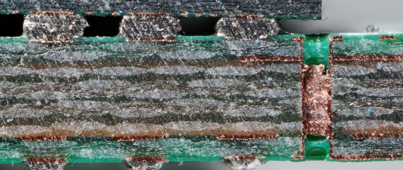
Via count only opens a local path. Temperature drops when via-wall copper, plane continuity, and the external cooling interface form one low-resistance thermal path.
A correct backdrill layer pair is only a logical definition. Stub length is set by stackup thickness, stop depth, oversize, and worst-case fabrication tolerance.
A via teardrop widens the joint root, but drill offset, etch, clearance, and flex can still leave a copper neck too narrow. Inspect the worst-case neck before release.
Intra-pair gap sets Zdiff on FR4; length matching does not fix an uncoupled route. Gap rules, delay match, and routing errors that still pass DFM.
Missing reference designators are often clipped where silkscreen enters a solder-mask opening. Use Silk To Solder Mask Clearance in DRC before fabrication.
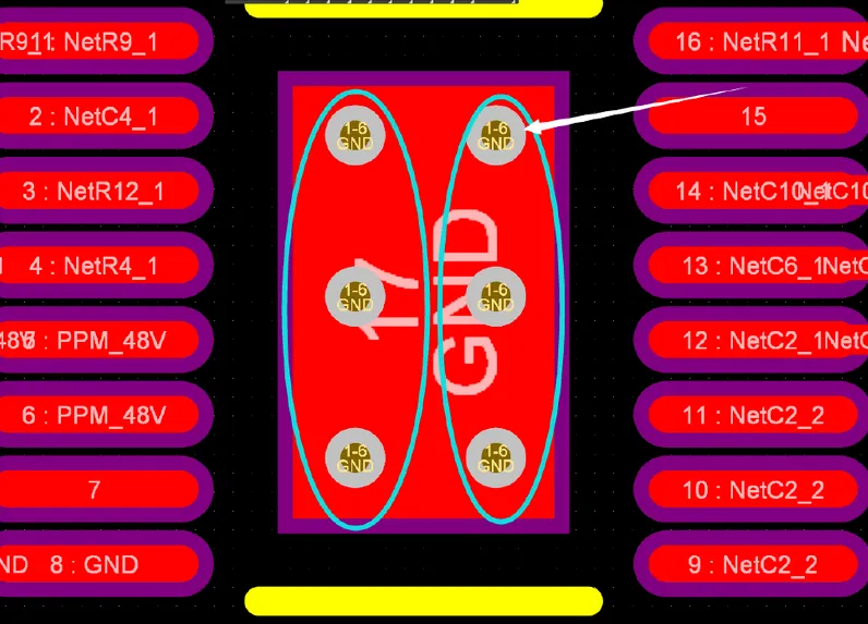
A GND net name does not mean copper is connected. Find isolated islands, thin necks, and fragments, then stitch or delete them so return paths stay controlled.
A small footprint origin shift can move an entire placement file. Align origin, pin 1, and zero-degree rules, then close the loop with one known part before export.
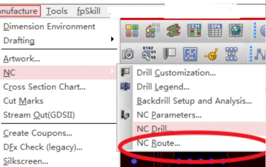
Drawing a slot on the mechanical layer does not define cutter path or plating. Align NC Route, pad attributes, and fab notes so CAM does not guess slot intent.
Learn how PCB anti-pad size affects via isolation, manufacturing clearance, plane continuity, and the risk of unintended connections in multilayer PCB designs.
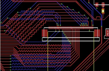
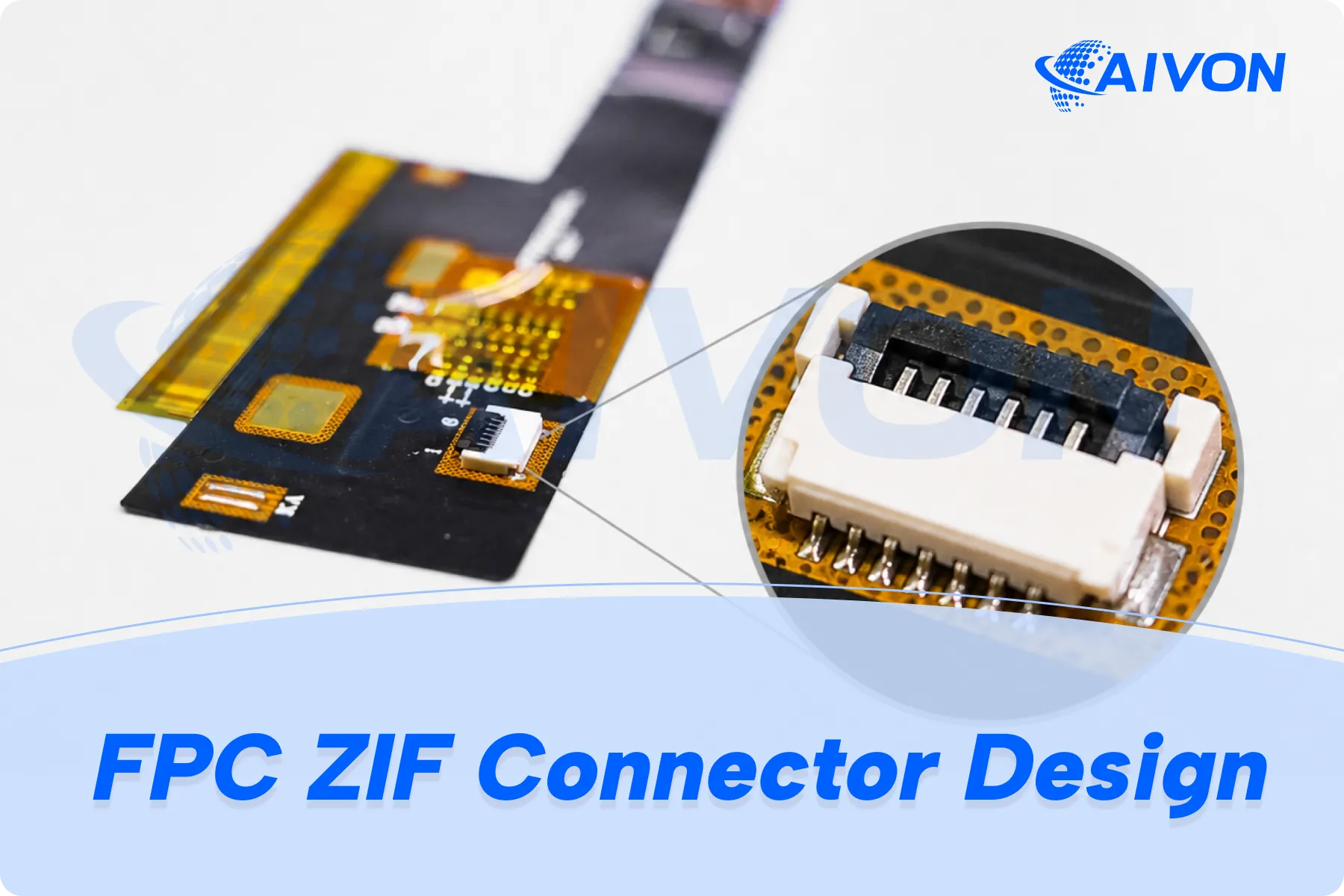
Engineering guide to FPC ZIF connector design covering ZIF vs LIF selection, PCB footprint rules, gold-finger plating considerations, mating-cycle factors, and approaches to reduce intermittent contact issues.
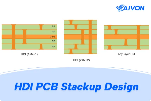
Learn how 1+N+1, 2+N+2, 3+N+3, and Any-layer HDI stackups differ in lamination, via strategy, yield, cost, and how to choose a manufacturable structure before layout freeze.