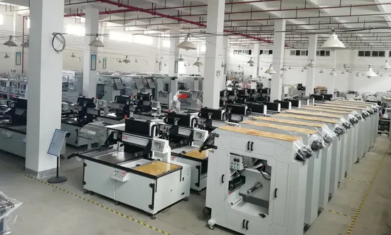
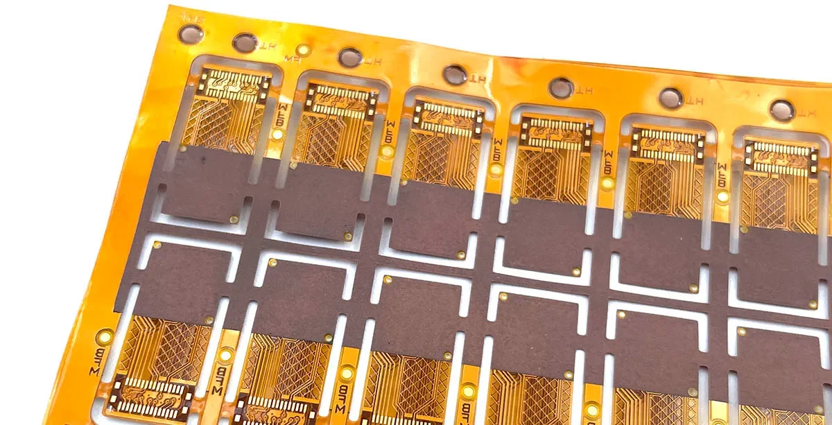
Coupons
Help
  • FAQ
    browse most common questions
  • Live Chat
    talk with our online service
  • Email
    contact your dedicated sales:
0

PCB Design

Printed Circuit Board (PCB) design forms the backbone of modern electronics, enabling the creation of compact, efficient, and reliable devices that power everything from smartphones to industrial machinery. In this category, readers gain access to a comprehensive collection of resources dedicated to mastering PCB design principles and techniques. Whether you are a seasoned engineer refining complex layouts or a newcomer learning the fundamentals, these articles provide the knowledge needed to tackle real-world challenges in electronics development. The scope of PCB design covered here extends from initial schematic capture to final board fabrication and testing. Articles delve into essential topics such as layer stacking, signal integrity, thermal management, and component placement strategies. Guides and tutorials offer step-by-step instructions for using popular software tools like Altium Designer and KiCad, while insights explore emerging trends like flexible PCBs and high-speed designs. Best practices emphasize error reduction, cost optimization, and compliance with industry standards, ensuring designs are not only functional but also manufacturable at scale. Real-world applications highlight the category's practical value, demonstrating how effective PCB design contributes to innovations in automotive systems, medical equipment, renewable energy solutions, and consumer gadgets. By addressing common pitfalls and sharing expert tips, these pieces equip professionals to enhance product performance and reliability. Readers benefit from building a deeper understanding through interconnected articles that cover foundational concepts alongside advanced methodologies, fostering continuous improvement in electronics projects. For those involved in prototyping or production, the technical relevance of this content lies in its focus on efficiency and innovation. Detailed discussions on impedance control, EMI shielding, and design for manufacturability prepare you to meet the demands of today's fast-paced tech landscape. Engaging with multiple articles in this category allows for a progressive learning path, where foundational knowledge supports exploration of specialized topics, ultimately leading to more robust and innovative PCB designs.

 
The Impact of Via Stub Length on High Frequency Signal Integrity
Signal Integrity High-Frequency PCB Impedance Discontinuity Via Stub Effect PCB Back Drilling High Frequency Design Multilayer PCB Design PCB Design For Manufacturing (DFM)

The Impact of Via Stub Length on High Frequency Signal Integrity

Via stub length drives resonance and high-frequency signal loss in multilayer PCBs, distorting signals through reflections. This article breaks down the via stub effect, S-parameter analysis, and proven fixes like backdrilling vias to minimize via stub length while boosting signal integrity for GHz applications.

PCB Impedance Control in Flex Circuits: Design Challenges and Solutions
Impedance Control PCB Reliability Rigid-Flex PCB High-Speed Design Polyimide PCBs Bend Radius Flex PCB Materials PCB Stackup Design

PCB Impedance Control in Flex Circuits: Design Challenges and Solutions

Tackle flex PCB impedance control challenges in flexible circuits with practical design solutions. Learn stackup optimization, hatched ground planes, bend radius management, and TDR verification to ensure signal integrity and reliability for high-speed applications. Ideal for electrical engineers. (198 characters)

PCB Impedance Control and EMI Reduction: Best Practices for Signal Integrity
Signal Integrity High-Speed PCB Impedance Control EMI Reduction PCB Thermal Design PCB Stackup Design Ground Plane Via Stitching Multilayer PCB Design

PCB Impedance Control and EMI Reduction: Best Practices for Signal Integrity

PCB EMI impedance control cuts emissions and boosts signal integrity in high-speed designs. Follow stackup optimization, routing techniques, grounding strategies, decoupling placement, and verification steps to minimize noise coupling, reflections, and compliance risks for reliable electrical engineering projects.

RF PCB Footprint Design: Optimizing for Performance and Minimal Loss
Design For Manufacturing (DFM) High-Frequency PCB Solder Joint Reliability Impedance Matching Via Stitching PCB Stackup Design RF Layout Low Loss Material

RF PCB Footprint Design: Optimizing for Performance and Minimal Loss

This guide explains RF PCB design techniques for footprints that ensure impedance matching and low loss performance. Electric engineers get structured principles on transmission lines, best practices like via stitching and simulations, troubleshooting tips, and standards for minimal signal loss in high-frequency boards.


2026 AIVON.COM All Rights Reserved
Intellectual Property Rights | Terms of Service | Privacy Policy | Refund Policy