










PCB Design
Printed Circuit Board (PCB) design forms the backbone of modern electronics, enabling the creation of compact, efficient, and reliable devices that power everything from smartphones to industrial machinery. In this category, readers gain access to a comprehensive collection of resources dedicated to mastering PCB design principles and techniques. Whether you are a seasoned engineer refining complex layouts or a newcomer learning the fundamentals, these articles provide the knowledge needed to tackle real-world challenges in electronics development. The scope of PCB design covered here extends from initial schematic capture to final board fabrication and testing. Articles delve into essential topics such as layer stacking, signal integrity, thermal management, and component placement strategies. Guides and tutorials offer step-by-step instructions for using popular software tools like Altium Designer and KiCad, while insights explore emerging trends like flexible PCBs and high-speed designs. Best practices emphasize error reduction, cost optimization, and compliance with industry standards, ensuring designs are not only functional but also manufacturable at scale. Real-world applications highlight the category's practical value, demonstrating how effective PCB design contributes to innovations in automotive systems, medical equipment, renewable energy solutions, and consumer gadgets. By addressing common pitfalls and sharing expert tips, these pieces equip professionals to enhance product performance and reliability. Readers benefit from building a deeper understanding through interconnected articles that cover foundational concepts alongside advanced methodologies, fostering continuous improvement in electronics projects. For those involved in prototyping or production, the technical relevance of this content lies in its focus on efficiency and innovation. Detailed discussions on impedance control, EMI shielding, and design for manufacturability prepare you to meet the demands of today's fast-paced tech landscape. Engaging with multiple articles in this category allows for a progressive learning path, where foundational knowledge supports exploration of specialized topics, ultimately leading to more robust and innovative PCB designs.
Latest Blogs

Signal Integrity vs. Power Integrity: Which Should Come First?
A practical engineering guide comparing signal integrity and power integrity, covering SI/PI modeling, PDN decoupling, DC IR drop, SSN, via-PDN interactions, and PCB design methods for robust high-speed systems.
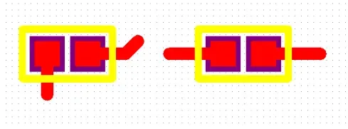
Practical Pad Naming Conventions in PCB Layout Libraries
Practical pad naming convention for PCB libraries: encode geometry in names to standardize SMD, through-hole, and thermal pads, enabling faster reviews and EDA automation.

Using Glass Fiber Mesh to Improve PCB Etching Speed and Uniformity
A practical engineering guide showing how a glass fiber mesh under a PCB improves etchant flow, speeds up etching, and enhances uniformity, with test observations, mechanisms, and safety tips.

Root Causes of Poor Signal Integrity in PCB Designs
An engineering analysis of why signal integrity degrades in digital systems, covering DC voltage drops, power and ground noise, crosstalk, reflections, and edge distortion, with determining factors and practical implications for PCB design.
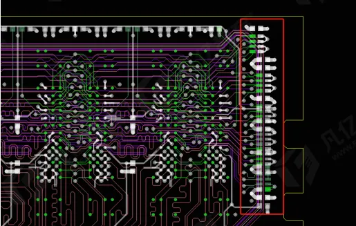
How Far from the Last DRAM Should the DDR End-Termination Resistor Be?
Practical analysis of DDR3 fly-by termination placement. Simulations at 533 MHz compare 100, 300, 500, and 1000 mil distances, showing why shorter end-termination segments improve eye diagrams and reduce overshoot/undershoot.
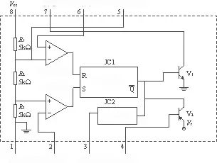
Common Protection Circuits for Power and Electronics: Overcurrent, Overvoltage, Overtemperature, No-Load, and Short-Circuit
Practical protection circuits for motors, inverters, lithium-ion chargers, and SMPS, including PTC-based thermal shutdown, reverse-battery and undervoltage protection, lithium battery protection ICs, and overcurrent methods using sense resistors, comparators, current transformers, and 555-based hiccup control.

How to Reduce Parasitic Capacitance in PCB Layout
Learn practical PCB layout techniques to reduce parasitic capacitance. Understand self vs. mutual capacitance, high dV/dt nodes, ground-plane proximity, and spacing to minimize capacitive crosstalk and noise.

Six Practical PCB Design Guidelines for Manufacturable, Reliable Boards
Practical PCB design guidelines focused on manufacturability and reliability: component placement, power/ground planes, routing, isolation, thermal reliefs, and ERC/DRC verification with illustrative examples.

15 Interesting NE555 Timer Circuits
Explore 15 practical NE555 circuits, from LED cubes and touch switches to servo testers, stepper controllers, and Zener testers, with design notes for robust, reliable builds.

Input Capacitor Current in DC/DC Buck Converters
Explains input capacitor RMS current in buck DC/DC converters, current sharing, ESR/ESL and MLCC bias effects, layout, and use of Power Stage Designer and TINA?TI.

PCB Parasitics That Affect EMI: What You Need to Know
How lead and via inductance and parallel-plane capacitance on PCBs drive EMI, with estimation methods and layout practices to reduce loop area and stabilize the PDN.
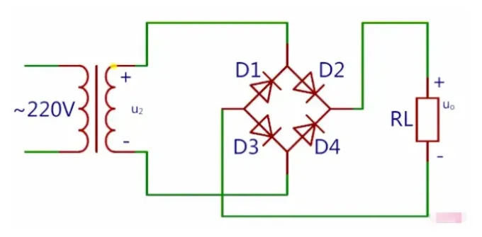
Bridge Rectifier Operation: Current Paths, Waveforms, and Practical Design Notes
Explains single-phase bridge rectifier conduction paths, full-wave output, DC about 0.9 Vrms, and how diode drops, ripple, and ratings influence component choice and PCB design.


