










PCB Design
Printed Circuit Board (PCB) design forms the backbone of modern electronics, enabling the creation of compact, efficient, and reliable devices that power everything from smartphones to industrial machinery. In this category, readers gain access to a comprehensive collection of resources dedicated to mastering PCB design principles and techniques. Whether you are a seasoned engineer refining complex layouts or a newcomer learning the fundamentals, these articles provide the knowledge needed to tackle real-world challenges in electronics development. The scope of PCB design covered here extends from initial schematic capture to final board fabrication and testing. Articles delve into essential topics such as layer stacking, signal integrity, thermal management, and component placement strategies. Guides and tutorials offer step-by-step instructions for using popular software tools like Altium Designer and KiCad, while insights explore emerging trends like flexible PCBs and high-speed designs. Best practices emphasize error reduction, cost optimization, and compliance with industry standards, ensuring designs are not only functional but also manufacturable at scale. Real-world applications highlight the category's practical value, demonstrating how effective PCB design contributes to innovations in automotive systems, medical equipment, renewable energy solutions, and consumer gadgets. By addressing common pitfalls and sharing expert tips, these pieces equip professionals to enhance product performance and reliability. Readers benefit from building a deeper understanding through interconnected articles that cover foundational concepts alongside advanced methodologies, fostering continuous improvement in electronics projects. For those involved in prototyping or production, the technical relevance of this content lies in its focus on efficiency and innovation. Detailed discussions on impedance control, EMI shielding, and design for manufacturability prepare you to meet the demands of today's fast-paced tech landscape. Engaging with multiple articles in this category allows for a progressive learning path, where foundational knowledge supports exploration of specialized topics, ultimately leading to more robust and innovative PCB designs.
Latest Blogs
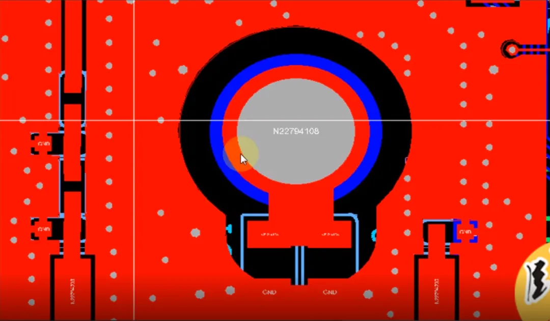
Why Designers Often Tie PCB Ground to Chassis Ground with a Parallel Resistor and Capacitor
Why tie PCB ground to chassis ground with a parallel RC network: operation, component values, layout practices, and test methods to improve EMI and ESD performance.
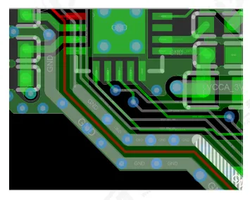
PCB Design Guidelines for Audio Interface Circuits
PCB design guidelines for audio interfaces covering clock damping, ground guarding, decoupling, I2S daisy-chains, SPDIF shielding, connector placement, and analog routing.
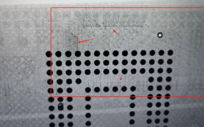
X-Ray Inspection of eMMC BGA: Solder Ball Assessment and an Unexpected Finding
X-ray inspection of eMMC BGA solder joints: evaluation of wetting, voids, and bridges; imaging revealed bond wires and an off-center die, with engineering review tips.
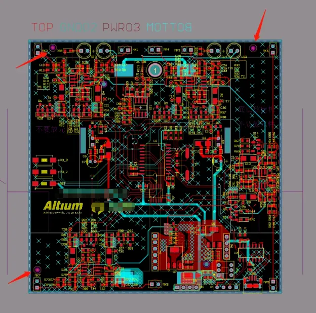
Why PCB Designs Include Fiducial Marks (Mark Points)
Overview of fiducial marks in PCB manufacturing: purpose, global vs. local types, geometry, placement rules, and SMT integration to improve accuracy and yield.
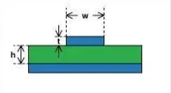
Classification and Differences of PCB Signal Traces: Microstrip and Stripline
Microstrip vs stripline in PCB design: field distribution, impedance control, EMI, loss, crosstalk, and stackup trade-offs for high-speed signal integrity.
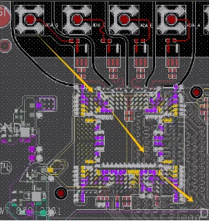
Mixed-Signal PCB Layout and Routing Design
Practical mixed-signal PCB layout guidelines covering analog/digital partitioning, grounding and return paths to reduce coupling and maintain signal and power integrity.
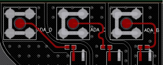
Mitigating Interference in Mixed-Signal PCB Design
Mixed-signal PCB design guidelines to mitigate digital-to-analog interference: grounding strategies, unified ground plane zoning, decoupling, and EMI-aware routing.
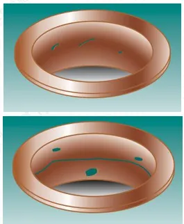
DFM Manufacturability Checks and Recommendations for PCBs
DFM checks for PCB design: open/short analysis, signal integrity, trace width/spacing, annular rings, via-in-pad, drill sizes, hole spacing, solder mask.
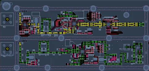
RF PCB Layout and Routing Essentials
Concise RF PCB layout and routing guidelines for 30 MHz–10 GHz: linear signal flow, shielding cans and via fences, 50 Ω controlled impedance, HPA/LNA isolation, antenna keepouts.
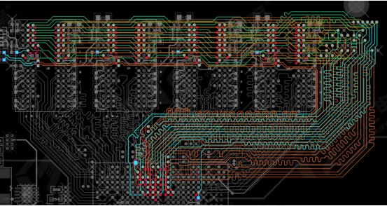
Detailed Analysis of DDR Topologies
Overview of DDR topologies—point-to-point, fly-by, and T-branch—covering advantages, signal integrity, termination, and timing calibration for DDR3/DDR4/DDR5.
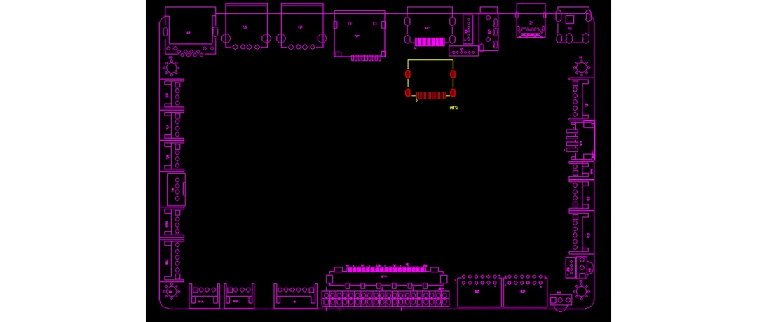
Why a Small Footprint-Origin Shift Moves Every Pick-and-Place Coordinate
How footprint origin, 0° baseline, and pin?1 orientation affect pick?and?place coordinates, and how to validate PCB/SMT placement data with a closed-loop check.

Seven Practical PCB Routing Rules for Reliable Layouts and Manufacturable Boards
Seven practical PCB routing rules to improve manufacturability, yield, and signal integrity: trace width, 45°/135° bends, avoid right angles, symmetric fan-out, connector breakout.


