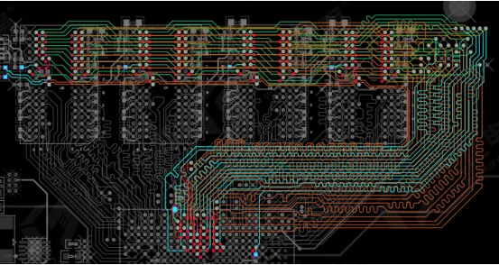
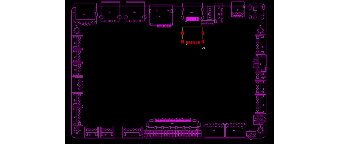
Radio frequency (RF) refers to electromagnetic waves in the range used for wireless communication. In PCB design, RF typically denotes analog signal paths from about 30 MHz up to 10 GHz. RF PCB design demands careful control of component placement, shielding, impedance, and coupling to ensure stable gain, low noise, and predictable performance across temperature and process variations.
RF Layout Requirements
-
Align the RF signal flow in a straight line within a single shield can. Within one shielding cavity, arrange the RF signal chain linearly along the primary signal flow. If space does not permit a straight line, an L-shaped path is acceptable. Avoid U-shaped topologies inside the same cavity because they increase feedback risk and cross-coupling by bringing outputs back near inputs and sensitive nodes. A linear or L-shaped arrangement minimizes unintended loop areas and reduces the likelihood of oscillation or desensitization.
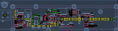
Figure 1 | Preferred linear or L-shaped RF signal flow inside a shield can to reduce feedback.
-
Keep identical RF channels identical in placement and routing. For systems with multiple receive or transmit channels, ensure each channel is placed and routed as symmetrically as possible. Matching length, topology, and component orientation helps maintain channel-to-channel gain, noise figure, and phase consistency, which is critical for beamforming, diversity, or any application requiring amplitude/phase matching.
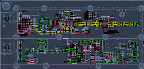
Figure 2 | Duplicate the placement and routing across channels to preserve matching.
-
Plan the main RF path and coupling control during placement. Place components by following the RF signal flow from input to output, while anticipating coupling between adjacent nodes (e.g., high-level outputs near low-level inputs, local oscillators near mixers, etc.). Use spacing, orientation, and shielding features to mitigate electric and magnetic coupling. When in doubt, rotate components and adjust spacing to reduce direct field overlap between sensitive nodes and aggressors.
-
Orient inductors to minimize mutual coupling. Inductive devices placed close together can couple magnetically, causing detuning and instability. Place adjacent inductors orthogonally (their axes at right angles) and increase spacing to reduce mutual inductance. Keep large inductors away from high-sensitivity resonant networks or low-level gain stages.
-
Isolate high-power amplifiers (HPA) from low-noise amplifiers (LNA). Keep transmit power amplifiers well separated from receive front ends. If PCB area is constrained, consider locating HPAs and LNAs on opposite sides of the PCB and, where feasible, operate them alternately rather than simultaneously to reduce self-interference. Where proximity cannot be avoided, reinforce isolation using shielding walls and via fences, and carefully manage return paths.
-
Partition RF modules with shielded cavities. Use shielding cans or partitions to isolate different RF blocks, especially between sensitive circuits and strong radiators. In multi-stage high-power amplifiers, separate stages to prevent interstage feedback and oscillation. Provide sufficient ground stitching around cavity boundaries to ensure low-impedance returns and robust shielding effectiveness.
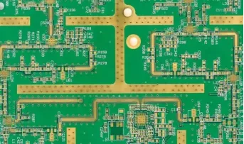
Figure 3 | Shielding partitions help isolate strong radiators from sensitive circuits.
-
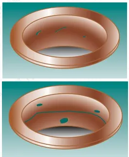
Add 3 mm plated mounting holes at the shield-can corners. Provide metallized holes in the corners of each shielding cavity to mechanically secure the shield and to create a low-impedance electrical bond between the shield and ground. Reliable mechanical contact improves RF continuity and reduces slot resonances along the shield perimeter.
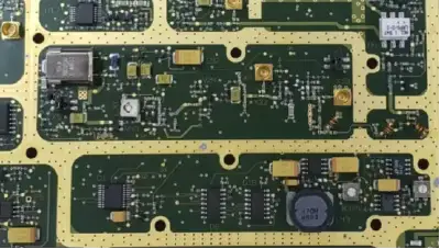
Figure 4 | Corner mounting holes ensure secure, low-impedance shield connections.
-
Prefer elongated shielding cavities; avoid square shapes. Increasing the length-to-width ratio of a shielding cavity helps spread resonant modes and reduces the likelihood that strong standing waves form at a single frequency. Square cavities are more prone to strong, discrete resonances that can couple into sensitive circuits and degrade performance.
RF Routing Requirements
-
Use 50 Ω controlled-impedance routing with rounded corners. Target a 50 Ω microstrip or coplanar-with-ground (CPWG) geometry based on the stackup, with a nearby reference plane to achieve the desired impedance with practical trace widths (often greater than 15 mil depending on dielectric thickness). Use arcs or well-mitered corners instead of sharp 90-degree turns to reduce impedance discontinuities and minimize reflection and radiation from corners.
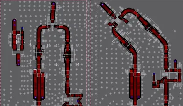
Figure 5 | Rounded or properly mitered corners maintain impedance and reduce corner radiation.
-
Maintain spacing and use via fences for isolation. Keep RF traces separated from adjacent ground copper by a spacing proportional to the trace width: a 2W clearance is recommended, with 1W as a minimum (W = the RF trace width). Use shielding via fences along critical runs; the center-to-center via pitch between the two rows should be less than 1/20 of the wavelength at the highest relevant frequency. As a practical guideline, a 60 mil pitch is commonly used, subject to performance and cost trade-offs. Also, for pads on the RF link that tie into ground copper, use solid connections (no thermal reliefs) to lower inductance and improve high-frequency grounding.
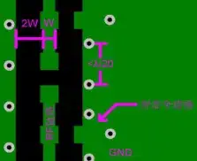
Figure 6 | Via fences increase isolation; keep via pitch small relative to the guided wavelength.
Note that the guided wavelength on the PCB is shorter than in air due to the dielectric; this makes the via spacing requirement more stringent at high frequencies. Consistent, closely spaced stitching vias provide a low-impedance ground return and suppress parallel-plate and slot resonances.
-
Separate digital and analog/RF domains; avoid monolithic power planes spanning both. Keep digital and analog sections isolated in both placement and copper pours to control return paths and coupling. Rather than a single, continuous power plane, use localized power islands or carefully segmented planes that align with the shielding cavities and return paths. Ensure that any necessary power-plane splits do not cut under RF traces or force long, indirect return currents.
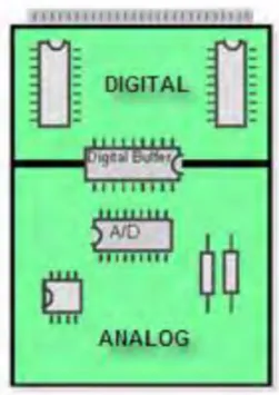
Figure 7 | Keep digital and analog/RF areas segregated; align power distribution with return paths.
-
Provide a continuous, via-free ground region in high-power areas. Ensure at least one solid ground region beneath high-power circuits to offer a low-inductance return and effective heat spreading. Avoid excessive vias or slots that break ground continuity in these regions, as they raise return-path inductance, increase loop area, and can fuel oscillations or spurious emissions.
-
Keep RF outputs away from RF inputs; add shielding if proximity is unavoidable. Physical separation reduces the chance that output energy couples back to the input, which can cause gain peaking, oscillation, or desensitization. If constraints force proximity, insert grounded shields, via fences, and orthogonal routing to suppress coupling, and ensure the return path for each stage is well-confined to its local cavity.
-
Route sensitive analog signals away from high-speed digital and RF aggressors. High dv/dt and di/dt edges in digital circuits, as well as strong RF carriers, can couple into low-level analog nodes. Maintain spacing, use grounded guard traces or planes where appropriate, and align return paths to minimize field overlap.
-
Manage copper geometry to avoid slivers and sharp points. Long, narrow copper slivers and sharp copper tips can act as unintended antennas or concentrate electric fields, promoting resonance and EMI. Where slivers are unavoidable, add two or more stitching vias along their length or at edges to tie them solidly to ground and damp resonances. Keep copper edges smooth and continuous wherever possible.
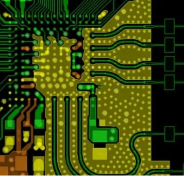
Figure 8 | Copper slivers should be minimized; stitch to ground to prevent resonance.
-
Maintain antenna keepouts across all layers. Keep all copper and components out of the antenna keepout region on every layer. As a practical guideline, maintain at least 5 mm clearance from the antenna area to minimize detuning and loss. Do not route traces beneath or near the antenna, and avoid placing ground fills that can perturb the antenna's radiation pattern or input match.
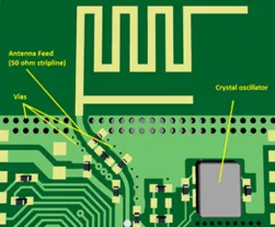
Figure 9 | A multilayer keepout around the antenna helps maintain efficiency and matching.
RF PCB design is an exercise in controlling fields and return currents as much as it is about placing components and drawing traces. Begin with a stackup that supports your target impedance and shielding strategy, place blocks to respect the RF signal flow, and partition cavities to confine currents and suppress coupling. With controlled impedance routing, disciplined shielding, and attention to copper geometry and return paths, RF layouts in the 30 MHz to 10 GHz range can achieve predictable gain, noise, and linearity with robust manufacturing margins.