End termination is a common and effective method to control reflections on DDR address and command nets routed in a fly-by (daisy-chain) topology. A practical question that often arises during layout is how far the end-termination resistor can be placed from the last DRAM device without degrading signal integrity. This article examines that placement question using a DDR3 fly-by case and time-domain simulations, focusing on the impact of the resistor-to-last-device distance on overshoot/undershoot and eye-diagram quality.
The prior analysis established that with a daisy-chain topology, the end of the chain requires a termination resistor to absorb the traveling wave and suppress reflections. Here, we specifically assess whether placing that resistor closer to or farther from the last DRAM yields better signal quality, and we quantify the trend by sweeping the placement distance.
Test Case and Simulation Setup
The case study uses a DDR3 fly-by topology connecting eight DRAM devices in series along the address/command bus. The devices are distributed along the chain, and the routing follows a standard fly-by arrangement from the controller to each device in turn. The analysis focuses on a single address line, A3, extracted as a representative net for the study. The stimulus toggles A3 at 533 MHz to emulate a realistic operating pattern and to excite the interconnect sufficiently for signal-integrity analysis. Measurements are taken at the receiver end of the last DRAM in the chain.
Key aspects of the setup include:
- Eight loads arranged in a fly-by topology along the address bus.
- Extraction of the A3 net for focused analysis.
- 533 MHz excitation to stress the interconnect and evaluate reflections, overshoot/undershoot, and eye metrics.
- End termination placed beyond the last DRAM with the distance from the last device to the resistor swept through several values.
The simulation compares four placement distances between the last DRAM and the termination resistor: 100 mil, 300 mil, 500 mil, and 1000 mil. For each case, the time-domain waveform and the eye diagram at the receiver end are evaluated.
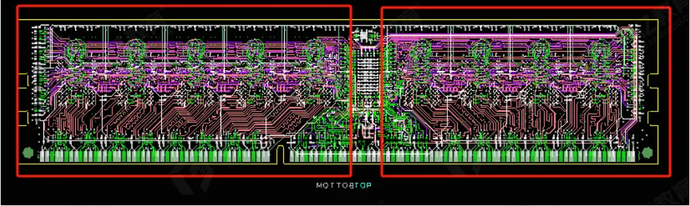
Figure | Board-level DDR3 fly-by (daisy-chain) concept
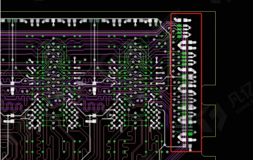
Figure | Representative routing/topology visualization
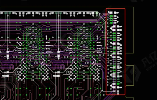
The A3 net topology is extracted from the board for simulation, isolating the relevant transmission-line sections, device pins, and the end-termination segment.
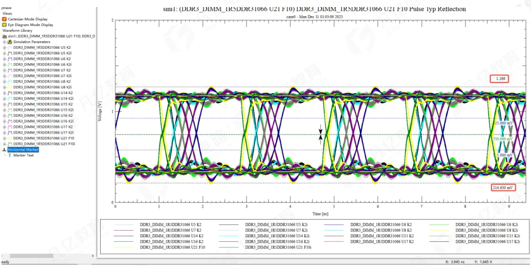
Figure | Measurement points and stimulus conditions
Results: Effect of Termination Distance
100 mil Distance
When the termination resistor is placed 100 mil from the last DRAM, the eye diagram at the receiver end is clear and well opened, with both eye width and eye height showing strong margins. Overshoot and undershoot are small. In general, the waveform indicates that the end-termination placement is effectively absorbing the residual energy with minimal additional interconnect between the last load and the termination.
Figure | Eye diagram with 100 mil resistor distance
300 mil Distance
Increasing the distance to 300 mil does not produce a significant deterioration in waveform quality for this case. Overshoot and undershoot remain modest, and the eye diagram continues to meet the target criteria. While the reflections increase slightly compared with the 100 mil case, the change is not large enough to push the eye beyond acceptable limits in this particular setup.
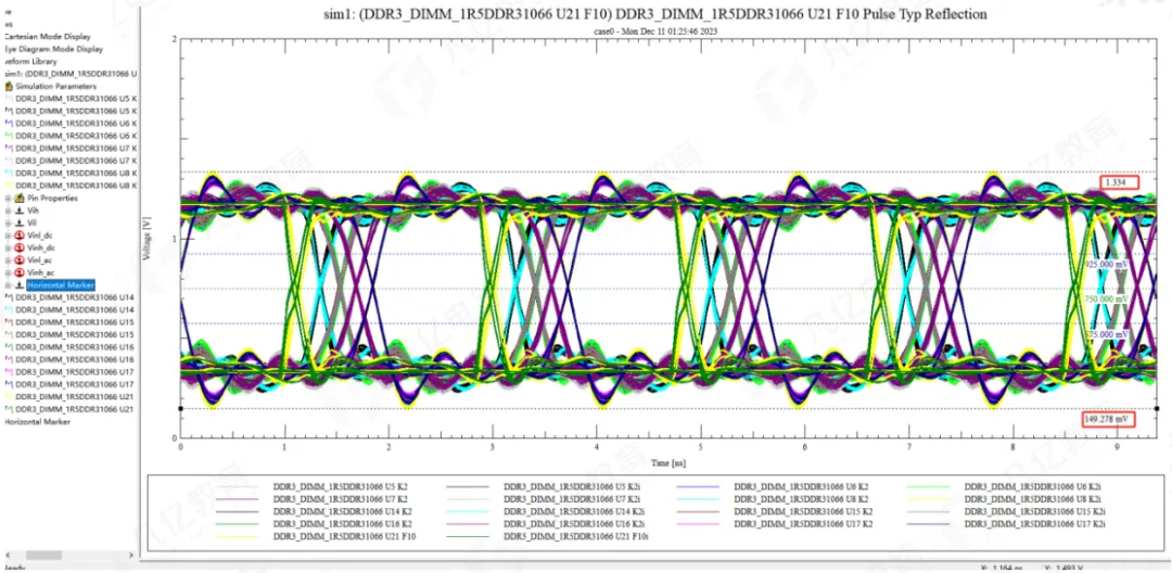
Figure | Eye diagram with 300 mil resistor distance
500 mil Distance
At 500 mil, the eye still meets the design goals in this configuration. However, a trend becomes clear: as the distance increases, both overshoot and undershoot gradually grow. The waveform exhibits more pronounced ringing and slower damping, which erodes eye height and width compared with the shorter-distance cases. Although the margins remain acceptable here, the degradation trend indicates reduced headroom against process-voltage-temperature (PVT) variations and manufacturing tolerances.
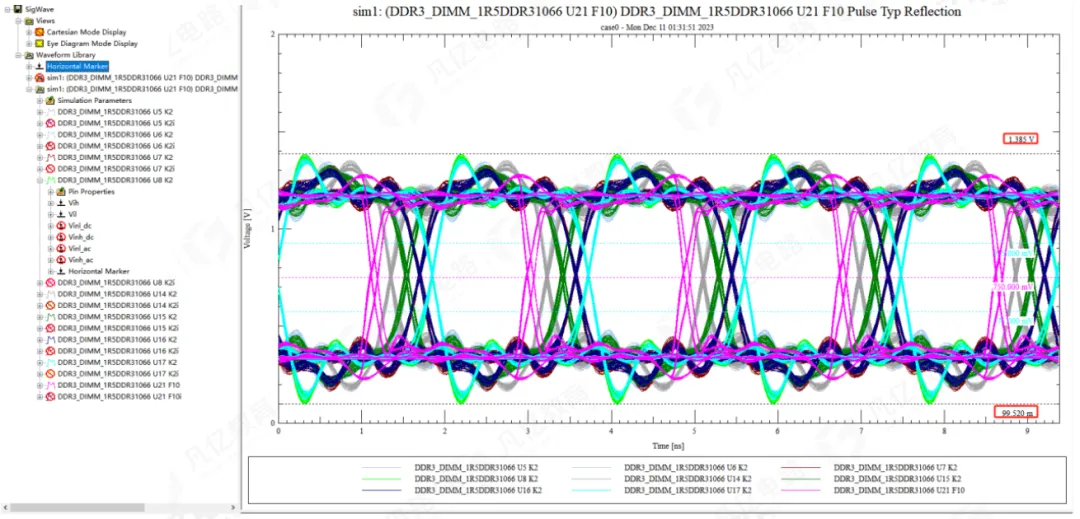
Figure | Eye diagram with 500 mil resistor distance
1000 mil Distance
With the distance extended to 1000 mil, overshoot and undershoot increase further, and the eye opening narrows in both time and voltage. The termination still provides some benefit compared with an unterminated end; however, the incremental effectiveness diminishes as the added length between the last device and the resistor grows. The eye remains analyzable, but the decreasing margin underscores that overly long end segments are counterproductive for robust designs.
Figure | Eye diagram with 1000 mil resistor distance
Why Closer Is Better: Transmission-Line Perspective
The observed trend is consistent with transmission-line behavior. In a fly-by topology, the termination is intended to absorb the forward-traveling wave at the end of the chain. If the resistor is placed a distance away from the last load, the trace segment between the last load and the termination acts as an additional transmission line. From the perspective of the last DRAM, that extra segment behaves like a stub leading to a termination.
When a signal step reaches the last device, part of the energy continues past the device into this end segment and is ultimately dissipated in the termination. However, the added segment has a finite propagation delay; during that time, the last device sees a temporarily mismatched load. The initial mismatch causes a reflection that returns toward the receiver and interacts with the main waveform. The longer the segment, the larger the round-trip delay and the more energy that can be stored and reflected, leading to more pronounced overshoot/undershoot and ringing.
As the segment length increases, the reflected components superimpose on the main signal later in time, often within the receiver sampling window. This reduces eye width (timing margin) and eye height (voltage margin). Beyond a certain length, the stub can form resonances related to the effective electrical length and rise time of the signal edges, which further exacerbates distortion. Placing the resistor as close as practical to the last DRAM minimizes the stub effect, reduces reflection amplitude, and improves damping, thereby stabilizing the eye diagram.
Design Guidance Derived from the Case
Based on the comparative simulations in this case, several practical conclusions can be drawn:
- Shorter is better. Placing the end-termination resistor closer to the last DRAM consistently yields cleaner waveforms, smaller overshoot/undershoot, and larger eye openings.
- Moderate distances may still pass. In this particular configuration, distances up to approximately 500 mil produced eye diagrams that met the criteria at 533 MHz excitation, though the waveform quality degraded gradually as distance increased.
- Long distances erode margin. At 1000 mil, both overshoot and undershoot increased noticeably, and eye margins shrank, indicating diminishing benefit from the termination due to the added stub length.
These observations align with common layout practice: keep the segment between the last device and the end termination as short as the placement and routing constraints allow. While the exact acceptable distance depends on the stack-up, trace impedance, device models, edge rates, and topology details, maintaining the resistor within several hundred mils of the last DRAM is a reasonable target in many designs, as it limits the stub length and preserves signal quality.
Implementation Tips for Layout and Verification
When implementing end termination for DDR address/command nets in a fly-by topology, the following considerations help translate the above behavior into robust designs:
- Minimize the end segment. Route the termination resistor as an in-line extension of the fly-by path rather than a long branch. Keep the distance from the last DRAM pad to the resistor pads as short as practical.
- Maintain controlled impedance. Ensure the short end segment uses the same reference plane and impedance as the main route, avoiding abrupt width changes or impedance discontinuities.
- Reduce via count. Each via adds discontinuity and additional delay; minimizing vias in the end segment reduces reflection and keeps the path electrically short.
- Avoid unnecessary meanders. Do not add length near the termination “just to match length” unless required by timing constraints and supported by SI analysis.
- Simulate what you build. Use the target stack-up and routing geometry to simulate the actual interconnect. Sweep the termination location in the model to quantify the impact on overshoot/undershoot and eye openings before finalizing placement.
- Validate with margins. Even if an intermediate distance passes in nominal simulation, consider PVT variations and manufacturing tolerances. Additional margin improves yield and robustness.
Summary
In a DDR3 fly-by topology, placing the end-termination resistor close to the last DRAM reduces the effective stub length, which in turn reduces reflections, minimizes overshoot/undershoot, and improves the eye diagram at the receiver. In the examined case, distances up to about 500 mil still produced compliant eyes at 533 MHz, though waveform quality degraded gradually with increasing distance. Longer distances, such as 1000 mil, further increased overshoot/undershoot and narrowed the eye, offering diminishing benefits from termination due to the added transmission-line segment.
For practical design, treat the end-termination placement as a controlled parameter and keep it as close as possible to the last device. Where constraints force a longer distance, verify the impact with simulation and ensure sufficient margin remains across expected variations. This approach balances layout flexibility with predictable signal integrity and robust DDR operation.