Introduction
Objective
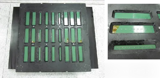
To improve plated through hole (PTH) hole-fill during wave soldering of DIP components, this study identifies the dominant factors affecting solder fill. We examine both the solder pallet (carrier) design and the PCB design, using a structured design of experiments (DOE) to quantify their impact on solderability.
Scope of Evaluation
The evaluation comprises a primary DOE and several secondary studies:
- Primary DOE: Six factors at three levels each, covering surface finish, PTH clearance, annular ring width, carrier aperture size, carrier aperture angle, and carrier-to-board contact area.
- Secondary studies:
- Effect of internal connection layer location on solder fill.
- Benefit of via-assisted connections versus direct PTH-to-copper connections.
- Effect of total connected copper cross-sectional area on solder fill.
Expected Outcome
The goal is to identify significant factors and optimal parameter ranges for solder fill across common PCB surface finishes and connected copper cross-sections. The resulting guidance supports design decisions and process adjustments. The results for connected copper cross-sections will also serve as a practical reference for current production limits.
Experimental Setup
PCB and Components
- Surface finishes: Three surface finishes were evaluated. ENIG (Electroless Nickel Immersion Gold), known for its favorable solderability in this context, was used as a control. OSP and LF-HASL boards were then assessed against the ENIG baseline.
- Estimated board and sample counts per production lot are shown below.
Component under test: Part number 09.1071D.25L (substitute: 09.1071D.A5L). Key specifications:
- Component diameter: 6.3 mm
- Lead pitch: 2.5 mm
- Lead diameter: 0.45 mm
- Lead finish: Ag-plated CP wire with Pb-free solder coating (Sn-3.0Ag-0.5Cu)
- Each PCB populated with 216 capacitors
Thermal Relief Pad Design
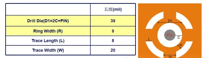
The thermal relief layout was based on the Hotshot capacitor thermal relief style. Fixed factors were trace length and trace width. The experimental factors were:
- Plated through hole diameter-to-pad clearance (PTH clearance)
- Annular ring width
Layer Stack and Connected Copper Cross-Section
The test vehicle was a 12-layer, 2.4 mm PCB. By varying internal copper thickness and layer connections, three total connected copper cross-sectional areas per PTH were created. The thermal relief design was applied consistently. The combinations were:
- Layers 8–12 connected: 336 mil2
- Layers 6–12 connected: 720 mil2
- Layers 1–12 connected: 1056 mil2
Reference: 1 oz copper thickness was 1.2 mil.
Primary DOE Factors and Levels
Factors were grouped into PCB design and carrier (solder pallet) design. The PCB design space comprised 3 × 3 × 3 = 27 combinations. The carrier design space comprised 3 × 2 = 6 combinations.
Secondary Experiments and Via-Assisted Design
The secondary studies evaluated:
- The impact of internal connection layer location (relative to the solder wave side) on hole fill.
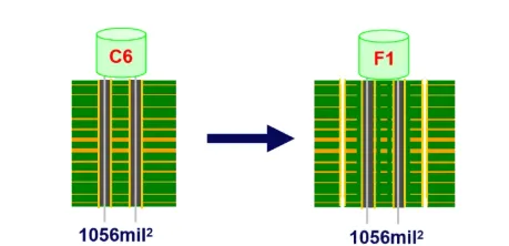
- Via-assisted design: When a PTH must connect to a large copper volume (e.g., all layers, 1056 mil2), direct connection can excessively sink heat and reduce solder fill. An alternative is to isolate the component PTH thermally and connect it to the large copper via a separate via on the bottom side, preserving electrical connectivity while improving solderability.
- The effect of total connected copper cross-sectional area.
Area F1 used the 1056 mil2 case to evaluate the via-assisted design for solder fill performance.
5D X-Ray Inspection
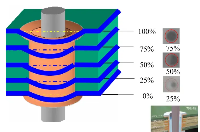
An HP 5D X-ray system was used to measure PTH hole fill for each pin. Each hole was analyzed at five axial slices. The average hole fill ratio was computed as the mean of the five slice areas.
Rework Test
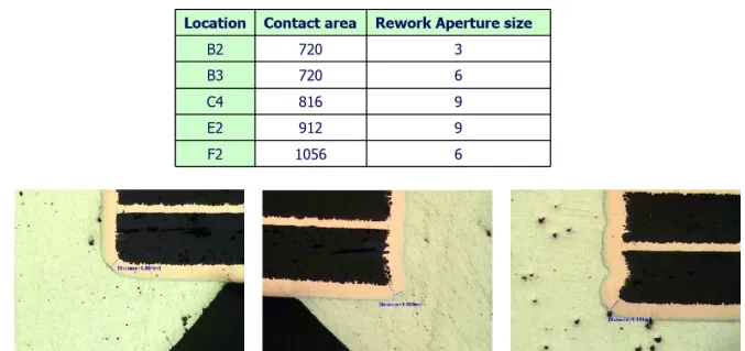
Representative boards from each surface finish (LF-HASL, OSP, ENIG) were selected for rework testing. Pads with clearance 11 mil and annular ring width 13 mil were cross-sectioned at locations B2, B3, C4, E2, F2 for evaluation. Hole fill and corner copper thickness were checked against criteria.
Results
SMT and DIP Process Time
Overall SMT and wave-solder timing used in the experiment is shown below.
SMT and Wave Solder Profiles
Thermal profiles for SMT and wave solder were recorded as the basis for comparing solder fill across factors and levels.
Primary DOE Findings
The DOE identified three dominant contributors to PTH hole fill: carrier contact area, PTH clearance, and carrier aperture size. These factors showed the largest contribution to variation in hole fill ratio. Two key observations:
- PTH clearance has a strong positive effect on hole fill. Two clearance specifications were in use; a single standard of 11 mil (single-sided) is recommended.
- For the PCB pad design, subsequent analyses use PTH clearance = 11 mil and annular ring width = 13 mil as the representative configuration.
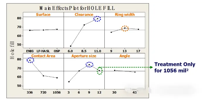
Among the tested factors, clearance and carrier aperture size exerted particularly strong influence on hole fill ratio. Larger aperture size improves hole fill, while larger carrier contact area reduces hole fill by sinking heat and restricting flow access.
Using the pad design with clearance 11 mil and ring width 13 mil, recommended carrier aperture values were derived against 75% and 50% process criteria. Trends observed:
- Hole fill increases with larger carrier aperture size.
- Hole fill decreases with larger carrier-to-board contact area.
- Design should reserve sufficient carrier aperture area according to the connected copper cross-section at each PTH.
Secondary Findings
Across secondary studies A and B, the same trend emerged: at approximately 912 mil2 of connected copper cross-section, hole fill dropped sharply. Based on the current equipment capability, 816 mil2 is identified as the practical limit to achieve the target hole fill in this configuration. The representative pad design used for analysis was clearance 11 mil and ring width 13 mil.
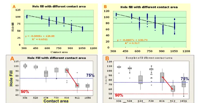
Connection layer location also mattered. With the same pad design (clearance 11 mil, ring width 13 mil), placing the large copper connection closer to the solder-wave side improved hole fill. The average hole fill ratio difference was about 25% in this test set.
Via-assisted design significantly improved solder fill for large copper attachments. For the 1056 mil2 case, connecting the large copper via a separate via increased hole fill by approximately 40% compared with directly tying the component PTH to the large copper.
Rework Results
For LF-HASL, OSP, and ENIG boards, the reworked pads (clearance 11 mil, ring width 13 mil) achieved at least 50% hole fill. Measured corner copper thickness at the bend ranged from 21 μm to 47 μm, satisfying the specification.
Experimental Limitations
- Estimated hole fill and DPPM are based on this test vehicle and equipment, and may deviate from mass production due to:
- Test board copper pour was uniform at 73.6%; mass-production boards vary in copper distribution and uniformity.
- The test board had no SMDs, which improves preheat effectiveness for DIP compared with typical assemblies.
- Layer connection patterns on the test board were more uniform than in mass production.
- 5D X-ray hole fill measurements are treated as reference values.
- Equipment and supplier variation.
- Directions for future improvement based on these results:
- Via-assisted designs showed significant solderability benefit; however, electrical characteristics must be evaluated jointly with design teams to meet both solderability and electrical requirements.
- Board temperature correlates positively with hole fill. Further experiments across different soldering machines should consider flux volatilization, residue, and component body temperature when optimizing profiles.
Conclusions
Primary DOE
- The combined contribution of connected copper area, PTH clearance, and carrier aperture area accounts for 83.56% of the hole fill variation.
- Contact area (carrier-to-board) is inversely proportional to hole fill.
- PTH clearance is proportional to hole fill.
- Carrier aperture size is proportional to hole fill.
- Reserve different carrier aperture sizes for different connected copper cross-sections during fixture design.
- PTH clearance: larger is better within the tested range. A unified specification of 11 mil (single-sided) is recommended. Annular ring widths of 9 mil vs 13 mil showed no significant difference; current designs may be retained.
Secondary Studies
- Even with a 9 mm carrier aperture, current wave-solder equipment cannot reliably achieve 50% hole fill when the connected copper cross-section exceeds 816 mil2.
- For large copper attachments, placing the connection closer to the soldering side yields about 15% higher hole fill compared with the component side in the summarized data set.
- When a large copper cross-section must be connected, place the connection on a layer near the solder-wave side.
- Via-assisted connection to large copper increases hole fill by roughly 40% compared with direct PTH-to-copper connection.
Rework Guidance
- Recommended pad design for robust rework: PTH clearance 11 mil; annular ring width 9 or 13 mil. These settings achieved ≥50% hole fill in rework while maintaining compliant corner copper thickness.
Glossary
-
PTH (Plated Through Hole): A through-hole on a PCB whose sidewalls are plated with metal to create an electrical and mechanical connection between layers.
-
Thermal Relief: A pad connection style using thermal spokes to a copper pour or plane to balance heat flow during soldering and prevent excessive heat sinking that degrades solderability.
-
SMD (Surface Mount Device): A component designed to be soldered directly onto the surface of a PCB without through-hole leads.
-
Spacing: The physical separation between features, components, or structures on a PCB or fixture.
-
DOE (Design of Experiments): A structured methodology for systematically exploring parameter spaces and quantifying factor effects and interactions.