


PCB Assembly
Printed circuit board (PCB) assembly represents a critical phase in electronics manufacturing, where components are mounted onto a board to create functional circuits. This process bridges design and production, ensuring that electronic devices perform reliably in diverse applications. From soldering techniques to component placement, PCB assembly encompasses the methods and technologies that transform bare boards into operational systems. Understanding these elements is essential for engineers, hobbyists, and industry professionals aiming to optimize production efficiency and product quality. Within this category, readers will find a comprehensive collection of guides that detail step-by-step assembly processes, tutorials on advanced tools like surface-mount technology and automated pick-and-place machines, and insights into troubleshooting common issues such as solder joint defects or thermal management challenges. Best practices are highlighted to promote reliability, including strategies for minimizing defects through quality control measures and adhering to industry standards like IPC guidelines. These resources draw from real-world expertise to address both fundamental concepts and cutting-edge innovations in the field. The practical value of mastering PCB assembly extends to numerous sectors, including consumer electronics, automotive systems, medical devices, and aerospace engineering. By applying the knowledge shared here, professionals can reduce manufacturing costs, accelerate time-to-market, and enhance device durability. For instance, effective assembly techniques ensure that circuits withstand environmental stresses, leading to longer-lasting products in demanding conditions. Delving into the articles in this PCB assembly category provides a pathway to deeper technical proficiency. Whether refining prototyping skills or scaling up production, the content equips readers with actionable strategies to tackle real-world challenges and stay ahead in an evolving industry.
Latest Blogs
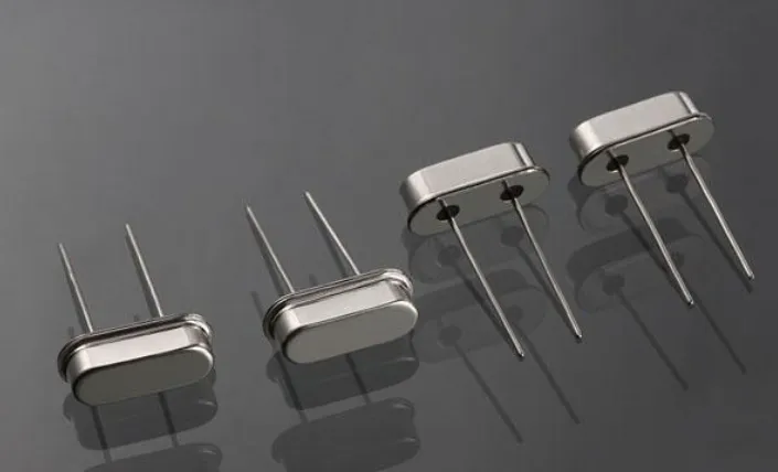
Crystal Selection for IoT: Balancing Size, Cost, and Performance
Master crystal selection for IoT devices with this practical guide. Learn how to balance small size crystals, low power consumption, frequency accuracy (±10–20 ppm), temperature stability, and cost for battery-powered sensors, wearables, and gateways. Includes selection matrix, PCB layout rules, load capacitor calculations, and real IoT case studies to avoid startup failures and extend battery life.
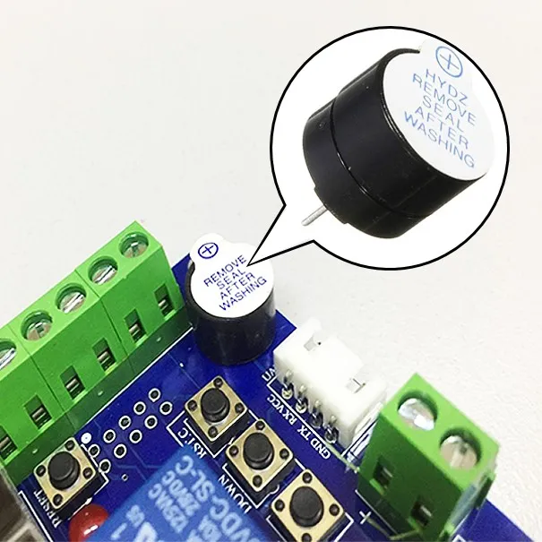
Extend Buzzer Life: Essential Tips for Engineers on Minimizing Failures
Electric engineers gain practical tips to improve buzzer reliability, prevent failures, and extend component lifespan. Optimize operating conditions, address environmental effects on buzzers, and apply PCB design and assembly best practices for durable performance.
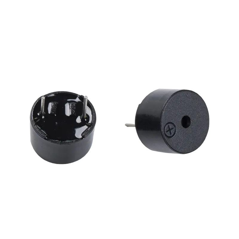
The Engineer's Guide to Piezo vs. Magnetic Buzzers: Choosing the Optimal Technology
Compare piezo buzzer vs magnetic buzzer for sound quality, power consumption, size comparison, and application suitability. This guide covers principles, key differences, and PCB integration best practices to select the right buzzer technology for electric engineers.
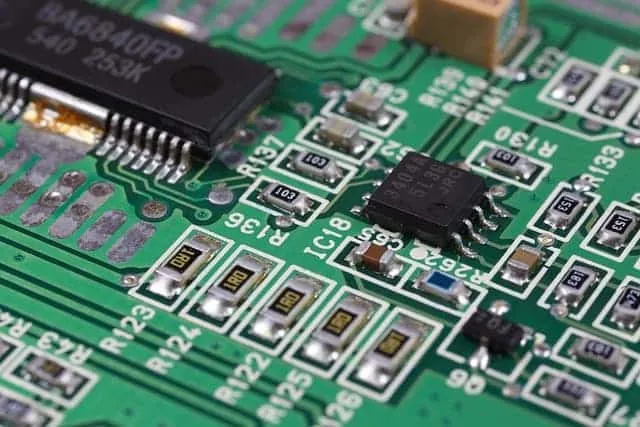
SMD Jumpers: Space Saving Solutions for High Density PCB Designs
SMD jumpers solve routing challenges in high-density PCB designs with compact, zero-ohm connections that save space and support automated assembly. Details cover SMD jumper advantages, design principles, footprints, current and voltage ratings, thermal options, and best practices aligned with IPC standards for reliable performance.
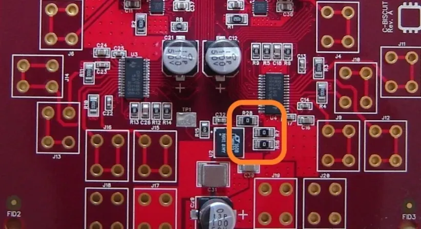
Zero Ohm Resistors vs. Jumpers: When to Use Which in Your PCB Design
Compare zero ohm resistor vs jumper for PCB design with details on applications, power ratings, SMT jumpers, routing tips, and selection criteria. Practical insights cover assembly compatibility, current handling, and reliability to fit your board layout needs in engineering projects.
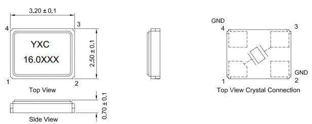
SMD Crystal Oscillators: A Comprehensive Guide to Surface Mount Technology
SMD crystal oscillators power precise timing in surface mount PCBs. Guide details package types like 3225 and 2016, advantages such as space savings and stability, applications in IoT telecom automotive, PCB layout best practices, reflow tips, and troubleshooting for engineers.
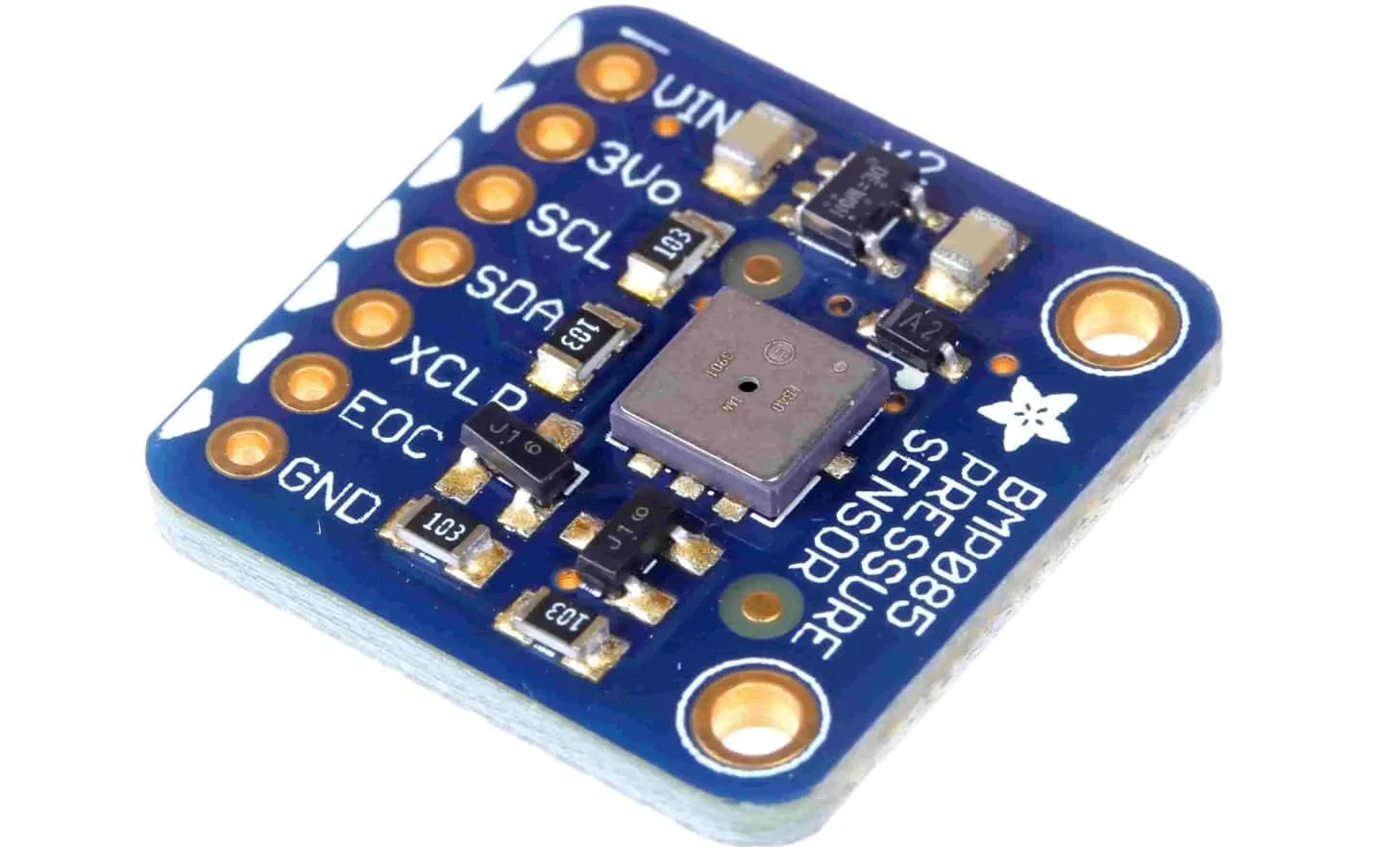
Pressure Sensors and IoT: Integrating Wireless Pressure Sensors with PCBs for Remote Monitoring
Integrate wireless pressure sensors with PCBs for IoT remote monitoring systems. This guide details data transmission protocols, power management strategies, PCB antenna design, security measures, and edge computing to build reliable sensor nodes for electric engineers.
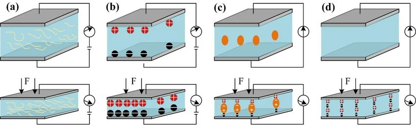
Enhancing PCB Performance: Optimizing Placement and Routing for Pressure Sensors
Follow pressure sensor placement guidelines and PCB routing techniques to improve signal integrity, reduce noise, and manage thermal issues. Learn decoupling capacitor placement, grounding techniques, and strategies for reliable sensor performance on high-density boards.
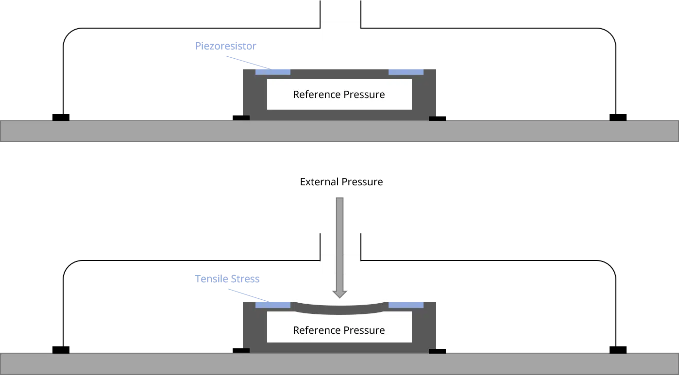
Navigating Pressure Sensor Selection: A Comprehensive Guide for PCB Integration
Pressure sensor selection criteria guide PCB integration success. Address design constraints, checklists, pressure range needs, signal options, footprint optimization, and environmental factors for reliable electric engineering designs and performance.
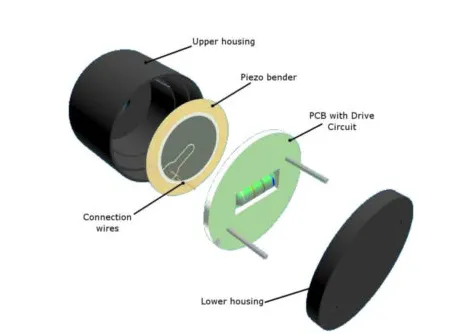
Buzzers in Automotive Electronics: Applications and Reliability Requirements
Automotive buzzer systems provide car buzzer alerts for safety features like seatbelts and parking sensors. Focus on buzzer reliability in vehicles through vibration resistance, automotive component standards, and testing. Practical guidance includes PCB mounting, integration tips, and fixes for common failures in harsh conditions.
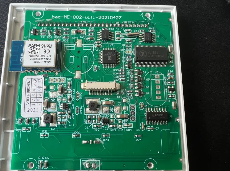
Surface Mount Current Sensors: Miniaturization Strategies for High Density PCB Assemblies
Integrate SMD current sensors into high density PCB assemblies with proven miniaturization strategies. Covers Hall effect principles, IPC land patterns, reflow soldering processes, layout tips, and troubleshooting defects for reliable surface mount current sensing in compact designs.
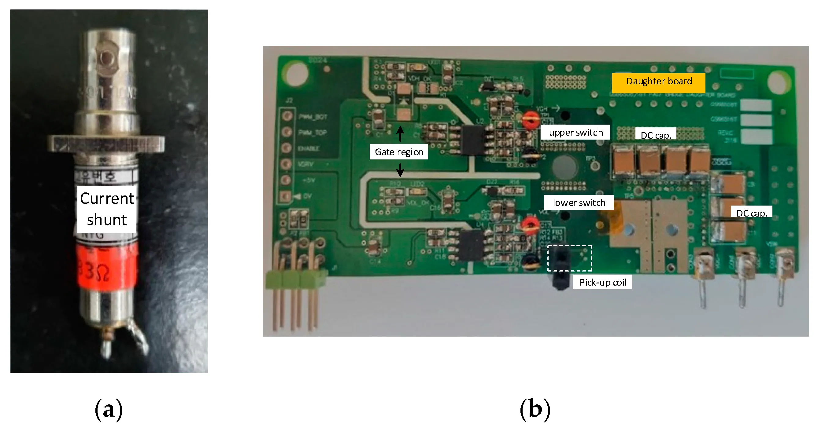
Isolated Current Sensors: Design Considerations for High Voltage PCB Applications
Examine isolated current sensor design for high voltage PCB applications. Details galvanic isolation, creepage and clearance distances, reinforced isolation strategies, layout techniques, and troubleshooting tips for safe, reliable power electronics.


