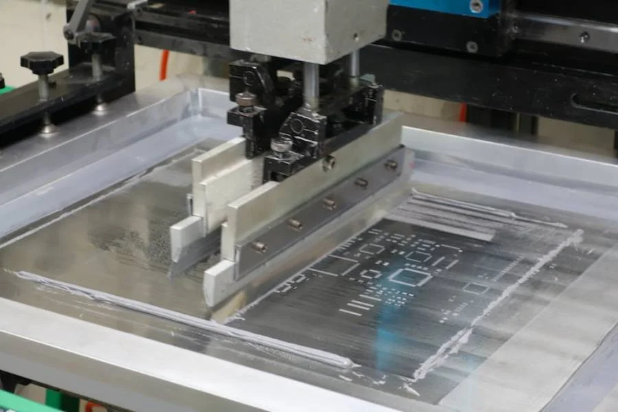
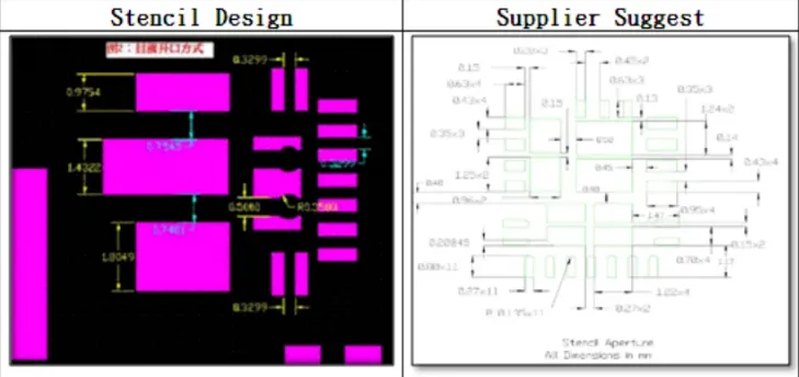
Solder paste printing is the first value-adding step in SMT assembly and a dominant driver of downstream reflow yield. The print defines the volume, shape, and placement of the molten solder that will ultimately form each joint. Small weaknesses in paste storage, stencil readiness, squeegee condition, PCB support, or inspection discipline can cascade into bridges, opens, insufficient solder, and skewed components. The following controls and practical considerations form a coherent process to stabilize solder paste behavior, maintain print repeatability, and improve SMT yield and efficiency.
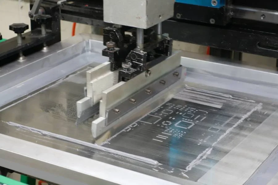
Figure 1 | SMT Stencil Printing Process
1. Solder Paste Storage and Use Control
Use a strict FIFO policy. Upon receipt, apply a Solder Paste Control label and store all jars at 2–8 °C. Prioritize consumption by expiry date and internal numbering. Before printing, allow the paste to warm up in a dry cabinet for more than 4 hours. Withdraw jars by ascending serial number and record each use in the solder paste control log.
Rationale: Temperature and time directly affect the paste's rheology and the flux's solvency and activation. Cold paste prints inconsistently; warming in a humidity-controlled environment prevents condensation (which can cause spattering and voiding) and stabilizes viscosity for consistent aperture filling and release. FIFO minimizes the risk of expired flux chemistry, which can lead to poor wetting and residues. Complete traceability in the control log supports lot-level defect correlation and rapid containment.
2. Refrigerator Temperature Control
Maintain refrigerators at 2–8 °C. If the temperature deviates, immediately execute the abnormal-temperature handling procedure and document it in the Refrigerator Temperature Abnormal Handling Record.
Rationale: Extended excursions can alter viscosity and oxidize the powder, degrading print definition and solderability. Lot quarantine and short-term process audits after excursions help prevent systemic defects.
3. Solder Paste Addition Control
- Predefine the printer's add-paste intervals based on the solder paste consumption per panel for the given product. When adding paste, confirm the bead size/quantity and document the action in the Solder Paste Inspection & Addition Record.
- Keep the plastic mixing/spatula blade clean to avoid contamination and dried paste lumps re-entering the bead.
- Use any opened jar within 24 hours. Unopened paste may be stored at room conditions for less than 1 month; beyond that, scrap the material.
Rationale: A stable bead height promotes uniform aperture filling and squeegee hydrodynamics. Dirty tools seed defects by transferring dried particles and oxides into fresh paste, clogging fine apertures and reducing transfer efficiency. Observing pot life prevents flux depletion and poor wetting, especially on fine-pitch and bottom-terminated components.
4. Stencil Control
4.1 Stencil Cleaning
Perform thorough stencil cleaning before starting a job, every 6 hours during production, and whenever the line has a cumulative stop of 30 minutes.
4.2 Post-Clean Inspection
After cleaning, inspect the stencil for paste residues on aperture walls and check for mechanical damage or wear (nicks, burrs, or dings), which impair gasketing and release.
4.3 Tension Control
After each up/down line or cleaning operation, measure stencil tension with a calibrated tension meter. The criteria are specified as ≤ -0.21 mm or ≥ 32 N/cm.
Rationale: Adequate tension ensures flatness and gasket integrity between stencil and PCB pads, sustaining print definition and preventing smearing or bridging. Loss of tension or frame deformation increases paste leakage and slumping, especially on fine-pitch patterns.
4.4 Stencil Life and Disposal
Retire the SMT stencil after 150,000 prints (counted as PCS/print) or immediately upon damage.
4.5 Stencil Cleaning Flow Control
Manage all stencil in/out and cleaning steps through the MES system for traceability and compliance.
Rationale: Proactive cleaning limits aperture clogging and paste build-up on the stencil underside, which otherwise cause insufficient or smeared deposits. Lifecycle control prevents quality drift from progressive wear.
5. PCB Positioning and Support
At changeover, set up the line according to the product specification package: flow direction, board dimensions, fiducial usage, and tooling. Ensure proper clamping and adequate PCB support under all critical print areas.
Rationale: Misalignment and board flex are primary drivers of paste offsets and uneven deposits. Rigid yet compliant supports under BGAs/QFNs and fine-pitch leads prevent local gaps at the stencil-to-pad interface. Good gasketing requires flat, stable contact to prevent paste bleed and bridging.
6. Squeegee Blade Control
- Use the MES system to control squeegee issue/return and on-line/off-line status for all operations.
- After removal from the line, clean blades and inspect for damage, burrs, or edge rounding.
- Replace blades after 150,000 prints or immediately upon damage.
Rationale: Blade edge quality and consistency strongly influence aperture filling, paste shearing, and roll dynamics. Worn or damaged edges reduce transfer efficiency and introduce directional print bias and streaking. Systematic tracking prevents extended use beyond effective life.
7. PCB Cleaning After Printing Exceptions
Clean PCBs when a printing/dispensing abnormality occurs, after a machine stop or incident requiring board rework, or when a PCB with printed paste sits more than 4 hours without completing reflow. Note: OSP-finished PCBs must not be cleaned directly with alcohol.
Rationale: Once flux solvents evaporate, the paste dries and no longer reflows as intended. Reprinting over partially dried deposits produces defects such as solder balls, voiding, and non-wetting. OSP is an organic protective layer; unsuitable solvents can degrade it, leading to oxidation and poor solderability. Use only approved cleaners and validated processes for the specific surface finish.
8. Solder Paste Printing Quality Control
8.1 SPI Inspection
When SPI is available, inspect every PCB automatically for thickness, area, volume, shorts, missing prints, and offset. Record the data for traceability and SPC.
8.2 Visual Control When SPI Is Unavailable
If SPI is not available or is down, implement operator sampling and visual inspection. Acceptable prints must exhibit no bridges, no missing deposits, and no misalignment, or an offset less than one-third of the pad width. Initiate a process deviation/temporary concession, secure approvals from responsible managers, and archive the record.
8.3 Paste Thickness and Volume Control Ranges
SPI measures volume as the primary control metric; thickness is used as an auxiliary reference. Recommended thickness reference ranges relative to stencil thickness (T) are:
- 0.5 mm pitch CSP / Micro BGA: T - 0.005 mm to T + 0.055 mm
- 0.5 mm pitch QFP / QFN: T - 0.005 mm to T + 0.055 mm
- 0.8–1.0 mm pitch BGA / CSP: T - 0.005 mm to T + 0.065 mm
- Normal chip (R/L/C and others): T - 0.005 mm to T + 0.085 mm
Remark: T = stencil thickness.
When controlling by SPI volume, the following reference ranges apply:
- 0.5 mm pitch CSP / Micro BGA: 0.0016387–0.008194 mm3
- CSP / Micro BGA 0.65–0.8 mm: 0.0065548–0.029497 mm3
- CSP / PBGA / Micro BGA 1.0 mm: 0.0163871–0.081935 mm3
- Other component volume controls: see the reference chart below.
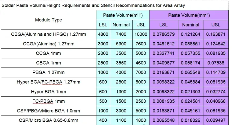
Figure 2 | Reference chart for solder paste volume control by component
When using SPI to verify print quality, operators must review and record the Cpk and average thickness every 2 hours.
Rationale: Volume correlates more directly with final joint geometry than thickness alone, especially for non-circular apertures and stencil reductions. The ranges above reflect practical allowances for transfer efficiency and release variability across pitches and component types, centered on the stencil thickness. Regular Cpk reviews identify drift and special-cause variation before defects accumulate, enabling timely corrective actions such as cleaning, tension checks, bead adjustment, or blade replacement.
Practical Links Between Controls and Yield
Each of the controls above targets a specific defect mechanism:
- Paste storage and warm-up prevent viscosity scatter and moisture uptake, reducing spatter, voids, and poor wetting.
- Scheduled addition and clean tools stabilize bead dynamics and aperture filling, limiting insufficients and local bridges.
- Stencil tension and cleanliness sustain gasketing and release, protecting fine-pitch definition and reducing bridging.
- Stable PCB support and alignment reduce offsets and smearing at the pad-stencil interface.
- Healthy squeegee edges preserve uniform shearing and transfer efficiency, improving consistency across the panel.
- SPI-based control and periodic Cpk checks catch process drift early, while documented deviations maintain accountability when SPI is unavailable.
- Timely PCB cleaning after anomalies avoids reflowing dried or contaminated paste, which often leads to solder balls and opens.
A disciplined, data-driven approach—combining FIFO material control, equipment condition management, environmental stability, and closed-loop SPI feedback—converts solder paste printing from a chronic source of variability into a predictable process. In turn, reflow defects decline, touch-up labor drops, and SMT line throughput and first-pass yield improve in a sustained, measurable way.
Note: Numerical ranges and life limits listed here apply to the specified conditions and categories. Always align control windows and acceptance criteria with your paste specification, stencil design, SPI capability, and product risk profile.
When the process is stable, incremental improvements—such as refining aperture designs, optimizing squeegee pressure and speed, or tuning under-stencil cleaning intervals—can be evaluated methodically using SPI distributions and Cpk trends to quantify the benefit without increasing rework risk.
Ultimately, solder paste printing performs at its best when the line runs as a single integrated system: controlled materials, controlled tooling, controlled machines, and controlled measurements. Get those pillars right, and yield follows.