When creating footprints in Cadence Allegro for QFN and similar packages with exposed thermal pads, many engineers run into the same question: “The datasheet shows a rectangular thermal pad with a slot or divided area. How do I build this irregular pad in Allegro when I can't find a matching template?”
This tutorial walks through a complete, practical workflow for creating irregular pads in Allegro using the Texas Instruments TPS54620 power device as an example. The process covers shape creation, solder mask and paste window definitions, and final integration in Pad Designer—illustrated step by step so you can replicate it with confidence.
Step 1: Review the Datasheet and Identify the Irregular Pad
Start by reviewing the device datasheet. For TPS54620, the exposed thermal pad in the center is not a simple rectangle. It incorporates a slot or divided area, which means a standard rectangular SMD pad won't suffice. You will need to define a custom pad shape that matches the recommended geometry.
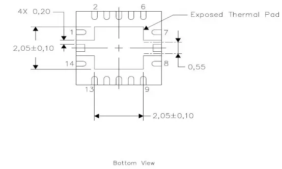
Figure 1 | TPS54620 package overview with an irregular thermal pad
Step 2: Extract Pad Dimensions from the Recommended Layout
Next, refer to the recommended PCB layout in the datasheet. The TPS54620 layout recommendation highlights the thermal pad dimensions in a red box. Use these dimensions as the authoritative reference for your shape: overall pad size, internal slot dimensions, and the width of the division channel.
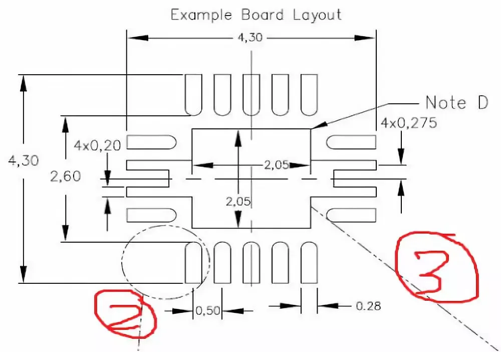
Figure 2 | Recommended board layout showing thermal pad dimensions
By combining the dimensional callouts (as shown in Figures 3 and 4), compile the data you will need to draw the pad shape:
- Overall thermal pad dimensions
- Dimensions of the internal slot or notch
- Width of the divided region
These will serve as the basis for building the custom Shape in Allegro.
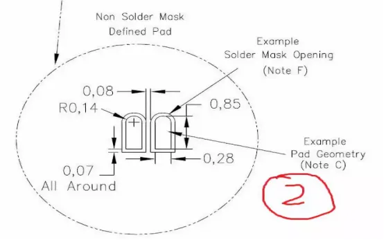
Figure 3 | Thermal pad dimension callouts (sheet 1)
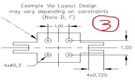
Figure 4 | Thermal pad dimension callouts (sheet 2)
Step 3: Create a New Shape for the Regular Pad in PCB Librarian
Open Allegro's PCB Librarian and create a new Shape file that will serve as the Regular Pad geometry. This Shape defines the copper pad outline.
- Menu: Shape → Add
- Select the appropriate Layer (typically Top)
- Enter the required dimensions and draw the outline per the datasheet
Because this Shape becomes the copper pad outline, it must precisely match the datasheet geometry.
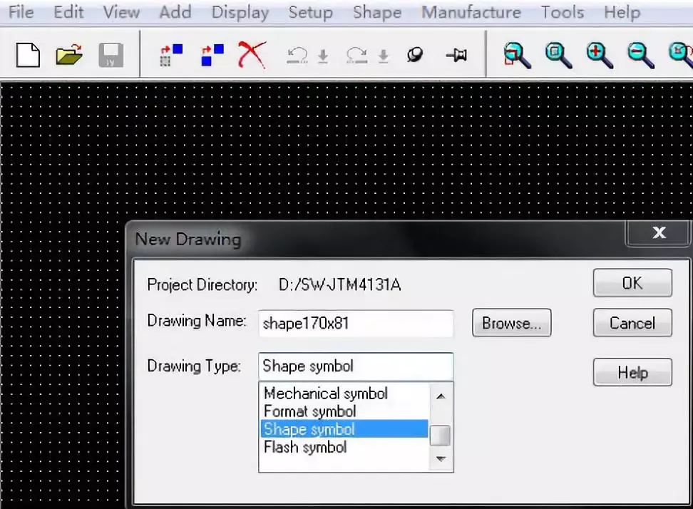
Figure 5 | Adding a Shape for the Regular Pad in PCB Librarian
Step 4: Draw the Symmetric Shape and Set the Origin
Draw the pad profile as a symmetric structure that matches the target geometry. In this example, a Shape named Shape170x81 was created to match the thermal pad dimensions. For ease of placement and alignment later, set the Shape's origin at the geometric center of the figure.

Figure 6 | Completed primary pad shape (Shape170x81) with center origin
Step 5: Create the Solder Mask Opening
With the copper Shape complete, create the solder mask opening for the pad. There are two approaches:
Method 1
- Redraw a new Shape and enlarge it by the required mask expansion (typically add 3–5 mil per side)
Method 2 (Recommended)
- Select the existing copper Shape and choose Edit → Z-Copy
- Set Type to Package to enable copying
- Apply a uniform offset or scale (for example, +6 mil) to create the mask expansion
- Delete the original if needed and keep only the enlarged copy
- Save the enlarged Shape as Shape176x87 and set its Type to Shape
This produces a solder mask opening Shape with a controlled expansion around the copper pad.
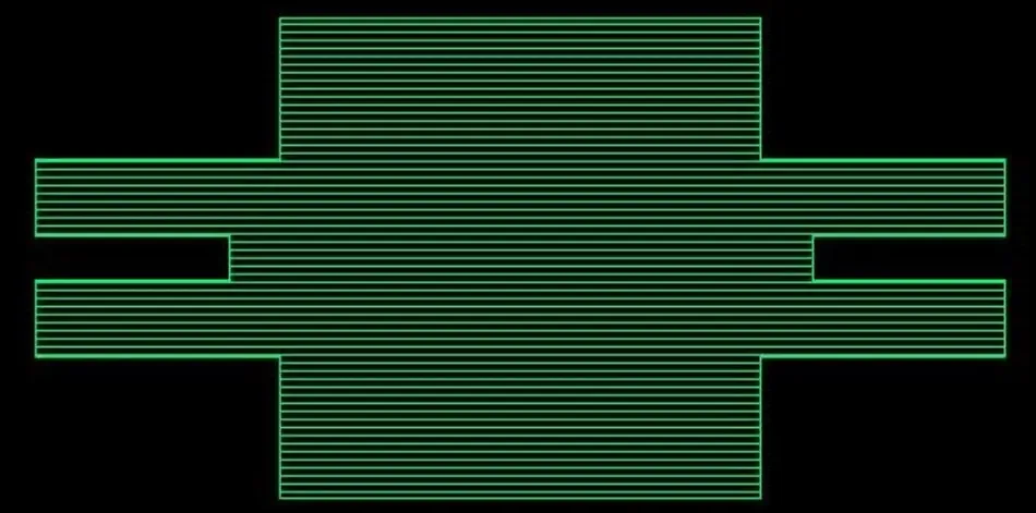
Figure 7 | Solder mask Shape created (Shape176x87)
Step 6: Define the Paste (Stencil) Openings
Create a Shape for the paste (stencil) layer using the datasheet's paste aperture recommendations. The paste windowing for large thermal pads is often segmented to control solder volume and improve voiding performance, so follow the datasource precisely.
- Refer to the paste opening dimensions (see Figure 8)
- Use the Edit → Z-Copy method to derive the paste Shape as appropriate
- Save the paste Shape, for example, as Shape170x81-P
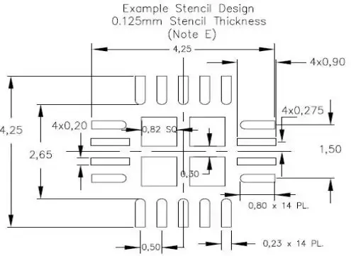
Figure 8 | Paste opening dimensions
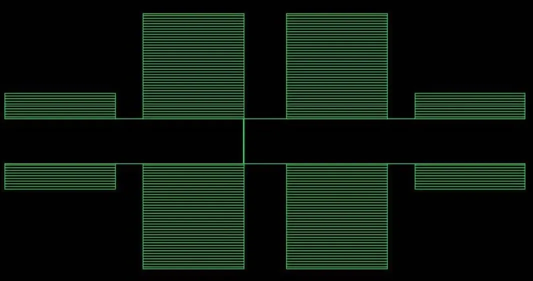
Figure 9 | Final paste layer shape (Shape170x81-P)
Step 7: Assemble the Irregular Pad in Pad Designer
Open Pad Designer and create a new SMD pad that references the three Shapes you prepared:
- In the Regular Pad Layer, load Shape170x81 (copper pad)
- In the Solder Mask Layer, load Shape176x87 (mask opening)
- In the Paste Mask Layer, load Shape170x81-P (paste aperture)
With these layers stacked, the three-dimensional definition of the irregular pad is complete.
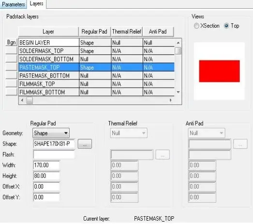
Figure 10 | Stacked Shapes in Pad Designer forming the irregular pad
Step 8: Save and Name the Pad
Save the completed SMD pad, for example, as smd170x81. This pad file can then be used directly when creating the final device footprint.
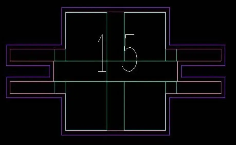
Figure 11 | Saved pad file (smd170x81)
Step 9: Apply the Pad and Build the Complete Footprint
Add the new pad to your device footprint. For the TPS54620 example, the complete QFN footprint (named QFN14_50-54620) references the irregular thermal pad you just created. This completes a production-ready package footprint, aligned with the datasheet's mechanical and assembly guidance.
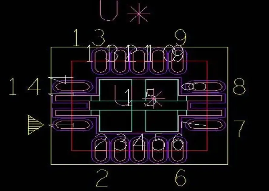
Figure 12 | Completed footprint (QFN14_50-54620) using the irregular thermal pad