Power design is one of the most critical and failure-prone parts of a PCB. Typical problems include overheating at power-up, unexpected interference despite seemingly clean routing, and confusion over how to place components from datasheet reference layouts. The good news: once you master a handful of core principles and can interpret the schematic correctly, you are already halfway to a robust design.
This article walks through practical, diagram-backed techniques for PCB layout of switching regulators and linear LDO regulators—from placement to copper pours, ground strategy, and via planning.
Basic Architecture of a Switching Regulator
A typical switching regulator module consists of:
- DC-DC converter core for power conversion
- Output sampling network (R1, R2) feeding the feedback comparator
- PWM error amplifier and gate driver that adjust duty cycle to regulate the output
The feedback divider compares the output voltage to the internal reference (Ur). The PWM controller modulates duty cycle to hold the output at the target voltage.
Switching Regulator PCB Design Guidelines
1. Start with the datasheet-recommended layout
After selecting the controller, download and study the datasheet. The vendor's recommended PCB layout is essential, especially the placement of key components such as input capacitors, output capacitors, inductors, MOSFETs, and the feedback network. Use it as your baseline and deviate only with clear justification.
2. Define the primary current path and prioritize placement around it
- Use the switching IC as the center of the placement and orient components according to its pinout.
- Do not place input and output filter capacitors side by side. Keep their current loops separate to prevent input noise from coupling into the output.
- Reserve copper area and via fields for high-current paths and thermal conduction.
In the illustration, the main current path is highlighted with thick traces. Pay attention to current flow direction and how copper pours collect and return that current.
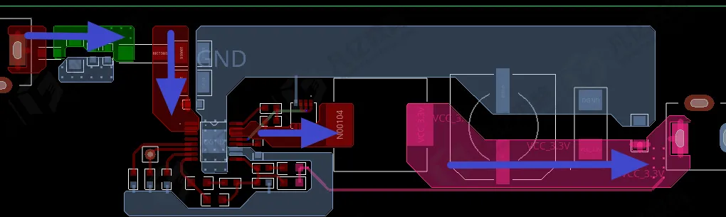
3. Favor a linear, compact "one-line" arrangement
- Place components in a neat, single-direction arrangement (a linear chain) aligned with the power flow.
- Minimize connection length and the number of vias on the primary power path.
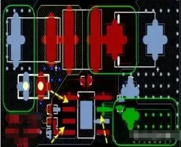
- Critical filter capacitors must be placed close to the relevant pins (see red boxes in the figure) and not scattered.
A compact layout reduces parasitics, lowers EMI, and improves thermal performance by shortening paths and minimizing loop area.
4. Route high-current paths with copper pours or wide traces
- Use wide traces or copper pours for common ground and for power input/output paths.
- For signal interconnects, use at least 10 mil width. Many engineers prefer 12–15 mil for robustness.
- Route high-current loops on the top or bottom layer to avoid fragmented current return paths and to improve thermal spreading.
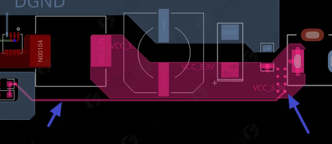
The following examples illustrate how trace width scales with current and how to treat high-current networks.
Figure 5 | Illustrative comparison of trace widths for different current levels.
5. Optimize SENSE, GATE, and INTVCC routing
SENSE line (voltage sense):
- Use approximately 0.5 mm trace width. Take the sense node from the output capacitor's load-side terminal rather than directly from the IC pin.
- Keep it away from high di/dt power nodes and switching inductors to reduce noise pickup.
GATE drive lines:
- Keep GATE routing as short and as wide as practical to reduce inductance and resistive loss.
- Avoid running GATE traces adjacent to high-frequency or sensitive signal lines to limit crosstalk.
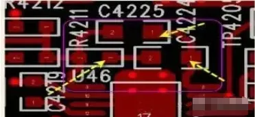
INTVCC decoupling:
- Place the INTVCC decoupling capacitor tight to the IC pins. This cap supplies GATE charge current and stabilizes the local supply.
- Provide a low-impedance return with short, wide connections to the IC ground pad.
Figure 9 | INTVCC decoupling must be close to the IC—keep loop area minimal.
6. No routing under the power pad or inductors; add thermal vias
- For packages with a power pad, open the solder mask over the pad, pour copper under it, and add a thermal via array to the ground plane for heat spreading.
- Do not route any signal under inductors. Avoid magnetic coupling into sensitive lines.
- For multi-output designs with adjacent inductors, orient inductors orthogonally to reduce mutual coupling.
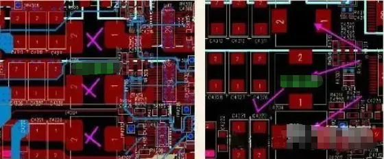
7. Copper pours: thermal reliefs and via stitching matter
- Do not connect every pad with solid copper. Use appropriate thermal reliefs to ensure solderability and avoid cold joints, tombstoning, and uneven solder build-up.
- Large copper areas must not rely on a single via to connect to ground. Use via arrays to lower impedance and improve both electrical and thermal performance.
LDO Design
LDO stands for Low Dropout Regulator—a linear regulator that maintains regulation with a small input-to-output voltage differential. It is well suited to low drop bucking such as 3.3 V to 1.8 V or 5 V to 3.3 V.
- Advantages: simple structure, fast start-up, low ripple, and stable output.
- Limitations: step-down only; typical output current does not exceed 2 A.
Layout essentials (example: 5 V to 3.3 V)
Place input/output capacitors close to pins:
- Place the bulk capacitor first (for example 10 μF), then add a small high-frequency capacitor (for example 0.1 μF) in parallel.
Make the main current path straight and wide:
- Use the shortest possible path to minimize additional voltage drop and to keep regulation tight.
Figure 12 | LDO placement with short main path and prioritized decoupling.
Ground routing for LDOs
- Connect the LDO ground pin to a generous ground copper area to increase conductive cross-section and heat spreading.
- Add multiple vias to ground; size and number should be consistent with the input/output current paths.
- Where practical, tie input and output grounds together nearby to form a tight loop and reduce noise.
The example highlights recommended copper width and via arrangement around the LDO.
Summary: Practical Differences at a Glance
| Design aspect | Switching regulator | LDO |
|---|---|---|
| Control method | PWM duty-cycle control | Linear control |
| Input/output placement | Linear "one-line" arrangement, capacitors close to IC pins | Place bulk first, then small HF capacitor, both near pins |
| High-current routing | Copper pours or ≥ 20 mil preferred for main paths | Widen the main current path |
| Ground strategy | Single-point grounding with multiple vias; tight high-current loops | Large ground copper with multiple vias; form a closed loop |
| Thermal guidance | Thermal via arrays and solder mask openings under power pad | Often no additional thermal measures needed, depending on load |
By applying these practices—prioritizing primary current paths, placing decoupling correctly, routing SENSE and GATE intelligently, using proper copper pours and thermal vias, and tailoring ground strategy to the regulator type—you can significantly improve power integrity, noise performance, and manufacturability in both switching and linear regulator designs.