In dense PCB designs, especially when the board is small and the component density is high, beginners often reach for a tempting shortcut: "If I can't fan out a trace, why not simply place a via right on the pad?" It sounds convenient, but this shortcut frequently leads to a long list of manufacturing and reliability problems: insufficient solder, voids and opens, tombstoning, pad lift, and painful rework.
This article explains why placing a via on a solder pad generally fails, where the risks come from, and in which limited cases it can be used effectively.
Why You Should Not Drill a Via on a Solder Pad
Traditional design rules treat via-in-pad as off-limits for most components. For BGA packages in particular, dropping a through-hole via directly in the pad can create severe assembly defects and long-term reliability issues. The primary failure mechanisms include:
- Solder paste wicking down the via during reflow, starving the joint on the pad and resulting in weak or open solder joints.
- Voids, partial wetting, or dewetting, which cause intermittent connections and costly rework.
- Pad deformation or pad lift, especially on small pads or thin copper, which can permanently damage the pad and degrade electrical performance.
At a physical level, an uncapped via acts as a capillary sink. During reflow, molten solder and flux are pulled into the via barrel by capillary action and outgassing. The pad sees a reduced solder volume, while the via's copper barrel absorbs heat and alters the local thermal profile. The result is an asymmetric wetting condition and insufficient solder at the pad where the joint must form. In fine-pitch BGAs, even slight solder volume loss can reduce standoff, collapse the solder ball unevenly, or trap voids under the pad. These mechanisms directly translate into assembly yield losses and latent field failures.
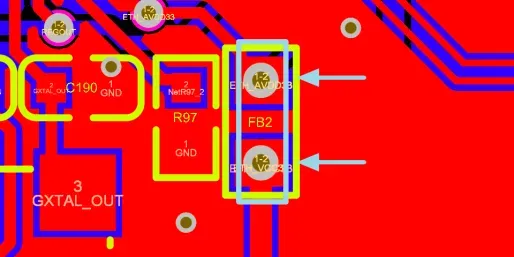
Figure 1 | A common beginner approach: via drilled on the solder pad
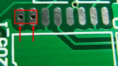
Figure 2 | Via-in-pad chosen due to limited space, but the hidden risks are significant
Historically, to avoid solder starvation and maintain robust solder joints, fanout traces were led away from the pad before transitioning into a via. This separates the soldering surface from the via and keeps molten solder localized to the pad during reflow.
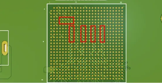
Figure 3 | Traditional approach: route away from the pad, then place the via
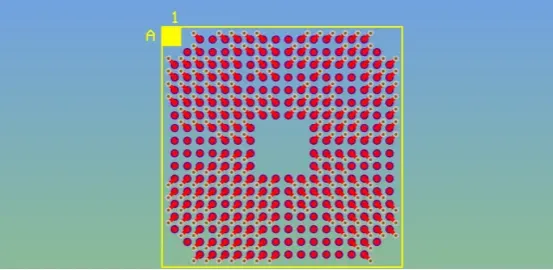
Figure 4 | Conventional layout avoids solder leakage by keeping vias off pads
Tombstoning: The Hidden Side Effect on Small Passives
Placing a via near or on the pad of small passives such as 0402 or 0201 resistors and capacitors can cause tombstoning during reflow. Tombstoning occurs when one end of a chip component lifts off the pad, standing upright like a "tombstone," typically due to unbalanced wetting forces and thermal gradients between the two ends.
When a via is placed at the edge of one pad, two things happen simultaneously:
- Solder paste volume is reduced on that side due to wicking, lowering the available solder to form a strong meniscus.
- The via increases the local heat capacity and can act as a heat sink, altering the reflow profile and causing one side to reflow earlier or later than the other.
The imbalance in solder volume and temperature profile translates directly into unequal wetting forces, making tombstoning much more likely on small chip components.
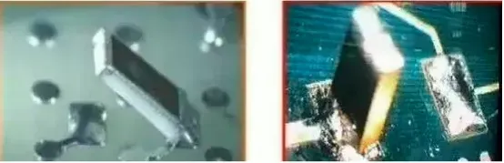
Figure 5 | Real-world example of tombstoning after reflow
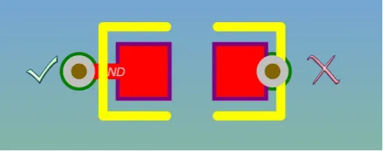
Figure 6 | Improper via placement near a pad creates unbalanced wetting forces
For small chip resistors and capacitors, do not place vias on or at the edge of the solder pad. Maintain a safe clearance between the via and the pad, keep paste apertures symmetric, and avoid thermal asymmetry between the two ends of the component.
When Is Via-in-Pad Acceptable?
While via-in-pad is not recommended in most cases, there are limited scenarios where it can be viable if the PCB stackup and manufacturing process are chosen carefully.
High-Density BGA Fanout with Blind/Buried Vias
When BGA pitch shrinks to 0.5 mm or below, conventional dog-bone fanout becomes impractical. In such cases, high-density interconnect (HDI) structures using blind and buried vias are often employed to escape routing:
- Blind via: a via that starts on an outer layer and ends on an inner layer without going through the entire board (for example, from the top layer to Layer 3).
- Buried via: a via that connects two inner layers and is not visible from the board surface.

Figure 7 | Blind via concept: outer layer to inner layer

Figure 8 | Buried via concept: inner-to-inner layer only

Figure 9 | Recommended HDI strategy for fine-pitch BGA with blind/buried vias
The tradeoff is cost and process complexity. HDI stackups require additional lamination cycles, laser microvias, and tighter process control, which increase fabrication cost. However, the benefit is that vias can be placed within tight footprints without creating solder starvation, provided they are implemented as blind/buried features and, where necessary, filled and capped to present a flat, solderable surface.
In any case where a via must be located on a solderable surface, use a filled and capped via process so the pad remains flat and sealed. Without fill and cap, via-in-pad will almost certainly wick solder during reflow and create opens or voids.
Disadvantages: higher cost and increased manufacturing complexity.
Thermal Via Arrays in Exposed Thermal Pads
Many ICs specify an exposed thermal pad under the package for heat removal. In these cases, the datasheet often recommends arrays of thermal vias inside the central pad to conduct heat into internal copper planes. These vias serve a thermal function rather than an electrical fanout function and do not involve leads or component terminations directly above them.
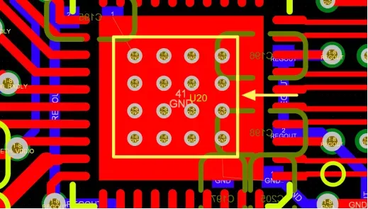
Figure 10 | Exposed thermal pad with thermal via array
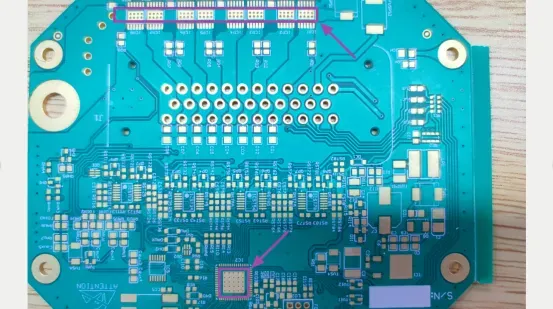
Figure 11 | Bottom of a leadless device; thermal vias do not affect lead solder joints
Because these vias are for heat conduction and the pad is not tied to a discrete lead, the tombstoning mechanisms described earlier do not apply. Follow the component's recommended pad and stencil design for paste coverage and via design, and you can safely use thermal vias within the exposed pad.
Practical Design Guidelines
To balance manufacturability, cost, and reliability, consider the following design practices:
- Do not place through vias on BGA solder pads. Use dog-bone fanout where space allows, or transition to HDI structures for fine pitch.
- For any via that must land on a solder surface, specify a filled and capped via so the pad remains flat, sealed, and solderable.
- Avoid placing vias at or near the edge of chip-component pads, especially for 0402/0201 sizes. Maintain clearance so the via cannot wick solder during reflow.
- Use solder mask dams between pads where possible to reduce solder bridging and control paste spread, and keep via annular rings fully masked or tented when they are near pads.
- Keep paste aperture designs symmetrical for paired pads to reduce wetting-force imbalance and tombstoning risk.
- For exposed thermal pads, follow the IC's datasheet for via count, diameter, and array pattern. These vias are for heat conduction and can be placed within the pad as recommended.
- Weigh the cost of HDI, blind/buried vias, and via-fill processes against assembly risk. For high-reliability products, the cost of robust via-in-pad implementation is generally justified by improved yield and field reliability.
Summary: It's Not Just About Layout Convenience
Via-in-pad yields serious assembly and reliability risks when used indiscriminately. In most cases, especially for BGAs and small chip components, keep vias off pads and maintain sound fanout and pad design practices. Reserve via-in-pad for specific, well-supported cases: fine-pitch HDI fanout using blind/buried vias with fill and cap, and thermal via arrays in exposed pads as specified by the component manufacturer.
| Scenario | Via on Pad Allowed? | Recommendation |
|---|---|---|
| BGA standard solder pad | Prohibited | Not recommended |
| Chip component pads (0402, 0201) | High tombstoning risk | Not recommended |
| HDI using blind/buried vias | Feasible | Acceptable with higher cost and process control |
| IC exposed thermal pad | Reasonable | Recommended per datasheet |
Design is a system-level decision. The placement of a via on a pad must consider assembly processes, reflow behavior, solder paste control, PCB fabrication capabilities, and long-term reliability. Treat via-in-pad as a specialized technique to be used with the right stackup and processes, not as a shortcut to patch routing challenges.