KiCad 10 will support flat, or tiled, schematic structures. Engineers who want to evaluate the feature before the stable release can try it in the 9.99 nightly build. The change addresses a long-standing workflow difference between KiCad and several commercial EDA tools: how additional schematic sheets are added to a project, and whether those sheets must live in a parent–child hierarchy.
For teams moving from other schematic editors, that difference is often one of the first sources of confusion. The project manager and the schematic editor do not present "add a peer sheet" as an obvious action. Historically that was not an oversight in the menus alone. KiCad only supported hierarchical schematics, so a new sheet had to be created as a child of an existing sheet.
Why Sheet Structure Matters When Switching Tools
In a hierarchical schematic, every additional sheet is introduced by drawing a hierarchical sheet symbol on a parent page and then opening that symbol to edit the child sheet. The relationship is explicit: one root, then nested blocks. That model works well when a design is partitioned as reusable blocks, when a sheet represents a repeated channel, or when the intent is to push ports through sheet pins.
It is less convenient when the design is simply large and the engineer wants several independent pages at the same level: power, MCU, analog front end, connectors, and so on, without wrapping each page in a sheet symbol. Tools such as Altium Designer and OrCAD commonly allow that flat, multi-page organization. Engineers coming from those environments expect to add a page, draw on it, and connect nets across pages with global or off-page names.
Until tiled sheets arrived, KiCad did not support a true peer structure. Newly created sheets could only form parent–child relationships. A widespread workaround was to keep a single top-level schematic and place multiple hierarchical sheet symbols on it, even when those symbols were not meant to represent nested functional blocks. Each symbol pointed at a separate sheet file. Connectivity between those sheets was then handled with global labels rather than sheet pins, because the sheets were not being used as true hierarchical modules.
That workaround is usable, but it is awkward. The top sheet becomes a parking area for unconnected sheet boxes. The project still looks hierarchical in the navigator even when the electrical intent is flat. Global labels carry the inter-sheet nets, which is easy to misuse if some nets were supposed to remain local. Designers who only wanted another page had to learn a hierarchical ritual that did not match how they thought about the design.
What Flat or Tiled Schematics Mean in KiCad
A flat or tiled structure treats multiple schematic pages as peers. There can be more than one top-level sheet. Those sheets sit side by side in the project rather than under a single Root page that must own every other file. Connectivity across pages still depends on consistent net naming, typically through global labels, but the project no longer requires dummy sheet symbols on a parent page just to attach extra files.
KiCad 10 is introducing this tiled structure so a project can be organized the way many engineers already partition boards: several top-level pages, each a complete drawing, without forcing a hierarchy that is only there to satisfy the file model. Hierarchical sheets remain available. The new capability is that hierarchy is no longer the only legal way to add a sheet.
KiCad 9.99 Nightly Preview
The behavior can be tested in 9.99 nightly builds from the KiCad download page nightlies section. Nightly builds are development snapshots. They are suitable for evaluation and issue reporting, not for treating a production database as if the file format were frozen.
The 9.99 file format is different from 9.0.x. If a design is opened and saved in 9.99, those files will no longer be readable by 9.0.x and cannot be reverted by simply reopening them in the stable 9.0 series. Back up the project—schematic files, board file, project file, and any associated libraries or simulation data—before using the nightly release on a design that must remain compatible with 9.0.x.
Behavior and UI in the preview
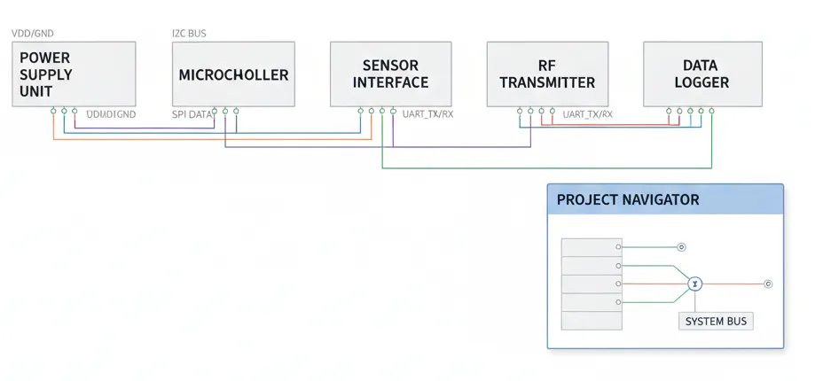
Figure 1 | Preview of tiled (flat) schematic sheets in KiCad 9.99 (nightly).
In the 9.99 preview, the schematic hierarchy can include multiple top-level sheets. Previously only a single Root sheet was allowed. That is the structural change behind tiled schematics: the project is no longer constrained to one top-level page with every other sheet hanging beneath it.
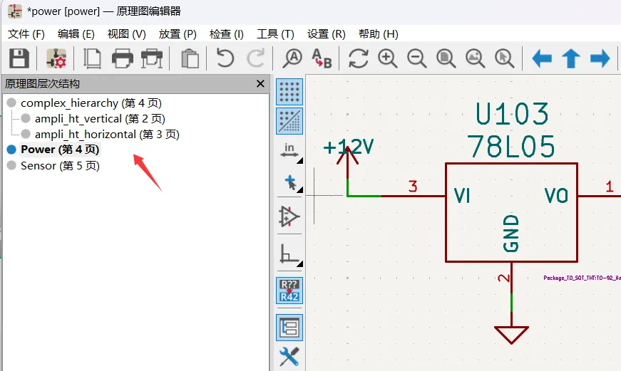
Figure 2 | Menu options for managing top-level pages in the schematic editor.
The schematic editor menu includes commands to add a top-level page and to remove a top-level page. Those actions operate on peer pages rather than on hierarchical sheet symbols drawn on an existing page. For a fully flat design, adding and removing top-level pages from the menu is enough to grow or shrink the page set.
When you add a top-level page and save, KiCad creates a new schematic file in the project folder:

Figure 3 | KiCad creates a separate schematic file for each added top-level page.
When a top-level page is added and the project is saved, KiCad creates a new schematic file in the project folder. Each top-level page remains its own file, which matches how KiCad already stores hierarchical child sheets as separate files, but without requiring a parent sheet symbol as the only way to introduce that file.
Mixing Flat Pages and Hierarchical Subsheets
A top-level page can still contain hierarchical subsheets. In principle, a project can combine several tiled top-level pages with nested sheets under one or more of those pages. That mix is possible in the preview, but it is not recommended as a default organization. Choose either a fully flat page set or a fully hierarchical tree unless there is a clear reason to combine both.
Mixing models makes navigation harder. The sheet tree no longer has a single obvious reading: some files are peers, others are children. Reviewers have to remember which nets are expected to cross through global labels between top-level pages and which nets are supposed to pass through hierarchical pins. For most designs, one convention is easier to teach, review, and maintain.
If the design is fully flat, keep connectivity rules consistent across the peer pages. Global labels that share a name are the same net. Local labels are not. That distinction existed in hierarchical KiCad projects as well, but it becomes the primary inter-page contract once sheet pins are no longer required to enter every additional page.
Testing Status
Tiled schematics are still in the testing stage in 9.99. Preview builds are the place to find broken menu states, unexpected file creation, navigator inconsistencies, or interactions with annotation, electrical rules, and netlisting. Report issues and suggestions during testing so fixes and workflow adjustments can land before the KiCad 10 stable release.
Because the file format already differs from 9.0.x, treat test projects as expendable or keep isolated copies. Do not assume that a workaround used in 9.0 hierarchical projects will map one-to-one onto multiple top-level pages until the release notes and the schematic editor have settled.
Other Features Expected in KiCad 10
Tiled schematics are not the only item associated with KiCad 10. The release is also reported to add assembly variants (Variant), X-Net (x-signal), and the ability to add PCB modules that can be synchronized with schematic modules.
Assembly variants matter on boards that share a layout but populate different options, voltage ranges, or regional builds. X-Net support matters when a logical signal spans multiple physical nets through series components, and those segments should be treated together for length, delay, or constraint purposes. Schematic-to-PCB module synchronization matters when a repeated block exists on both the schematic and the board and should stay aligned as the block is edited.
Those items sit alongside flat sheets as workflow features: they reduce the need for tool-specific workarounds that experienced users of other EDA systems already expect. They should still be validated in nightly or release-candidate builds rather than assumed complete from preview descriptions.
Practical Takeaway
KiCad 10's tiled schematic support removes the requirement that every extra sheet be born as a hierarchical child. Multiple top-level pages, menu commands to add and remove those pages, and a new schematic file per page give a flat project structure that is closer to common commercial-tool practice. Hierarchical sheets remain available; the improvement is that hierarchy is no longer mandatory for multi-sheet projects.
Use 9.99 only with backups. Keep a project either flat or hierarchical unless mixed structure is deliberate. File issues found in the nightly so the stable KiCad 10 behavior is driven by actual schematic workflow, not by the old single-Root limitation.
Credit belongs to the KiCad community developers for continuing to extend the toolset with features that simplify how electronics designs are partitioned and edited.