Robust PCB layout is a combination of disciplined planning, constraint-driven execution, and careful verification. A layout that meets signal-integrity (SI) and power-integrity (PI) requirements, is manufacturable, and performs reliably in the target environment depends on a coherent approach from stackup definition through routing and documentation. This article distills practical techniques that help engineers deliver repeatable results across a wide range of designs.
Plan the Stackup and Constraints Upfront
Effective layouts start with a well-defined layer stackup and explicit constraints. Decide early how many signal and reference layers are required, where solid ground and power references will be placed, and which layers will carry controlled-impedance traces. Align this with board thickness, dielectric choices, and achievable manufacturing tolerances to ensure impedance control.
- Define controlled-impedance layers: Identify which layers will be used for high-speed single-ended and differential routes. Coordinate trace width, spacing, and dielectric thickness with the manufacturer.
- Assign stable reference planes: Provide continuous ground planes under high-speed and sensitive signals. Avoid splitting ground planes under critical routes, and ensure power planes have defined return paths.
- Select via technologies: Decide where through-hole vias, blind/buried vias, or microvias are needed for escape routing, density, and SI. Understand the inductance impact of each via type.
- Capture constraints in the tool: Encode impedance targets, length-matching budgets, differential pair rules, spacing, and clearance in the design rules to enforce consistency across the layout.
Placement Strategy Driven by Function and Flow
Component placement sets the stage for signal quality and routing efficiency. Group components by function, align the flow of signals, and position critical elements to minimize loop areas and path length.
- Partition by function: Separate high-speed digital, sensitive analog, RF, and power sections. Provide appropriate keepouts and guard regions between domains.
- Short and direct critical paths: Locate timing-critical devices (e.g., clocks, memory interfaces, high-speed transceivers) to minimize path length and skew.
- Respect orientation and symmetry: Maintain consistent orientation for connectors and large ICs when it helps align breakouts and reduce crossovers.
- Consider thermal and mechanical factors: Place heat-generating components for effective cooling, and align heavy parts with mechanical supports to manage stress and warpage.
Power Distribution Network and Decoupling
A stable power distribution network (PDN) is the foundation for signal integrity. The objective is to deliver low-impedance power across the frequency spectrum while minimizing loop area and mounting inductance.
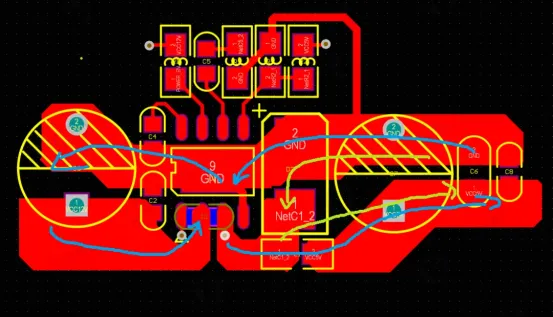
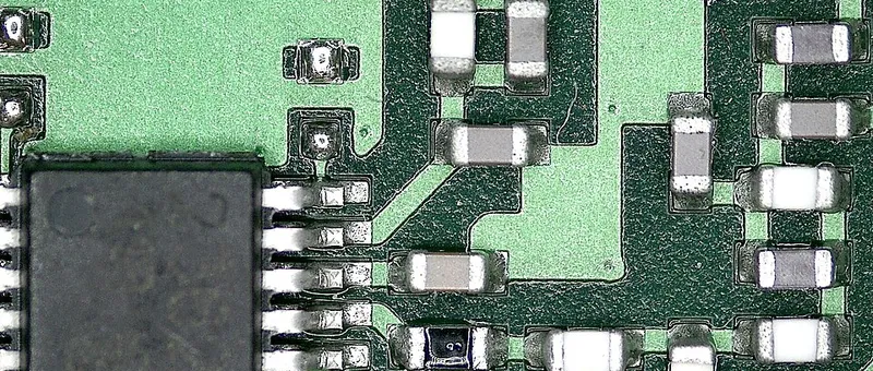
- Place decoupling capacitors close: Position capacitors as close as possible to IC power pins, with short, wide connections to the power and ground planes to reduce series inductance.
- Use a range of capacitances: Combine bulk, mid, and high-frequency decoupling to cover the device’s dynamic current needs. The exact mix depends on device requirements and board constraints.
- Minimize loop area: Keep the loop between capacitor, power pin, and ground return compact. When possible, use direct vias to planes adjacent to the component layer.
- Provide continuous return paths: Maintain uninterrupted ground references beneath power and signal routes so return currents can follow their natural paths without detours that raise impedance.
High-Speed Signal Integrity Practices
Routing high-speed signals as transmission lines with controlled impedance is critical for preserving waveform fidelity and timing margins. The following practices help manage reflections, skew, and loss.
- Control impedance and geometry: Use consistent trace widths, spacings, and reference plane distances that meet target impedances. Avoid sudden neck-downs or geometric changes that create impedance discontinuities.
- Length matching within budgets: For buses and differential pairs, adhere to the specified intra-pair and inter-signal length-matching tolerances. Keep serpentine tuning compact and avoid excessive meanders that add loss or crosstalk.
- Preserve differential pair coupling: Route pairs together with consistent spacing, length, and environment. Avoid splitting the pair around obstacles or changing reference planes without planning for the impact on impedance and return paths.
- Manage via transitions: Each via adds discontinuity and inductance. Minimize the number of layer changes for critical signals, and place return vias near signal vias to give return currents a direct path when crossing reference planes.
- Maintain clean reference transitions: When a signal moves between layers with different reference planes, provide stitching or return vias to bridge planes and keep return current continuity.
Return Path Continuity and Plane Integrity
Signal quality is as much about the return path as the forward path. Any disruption in the return plane forces currents to detour, increasing loop area, radiated emission, and susceptibility to noise.
- Avoid crossing plane splits: Do not route high-speed or sensitive signals across gaps in reference planes. If unavoidable, provide a stitched bridge or redesign the split boundaries.
- Use stitching vias near discontinuities: Place ground stitching vias along the edges of plane changes, near layer transitions, and beside high-speed paths to offer low-impedance return paths.
- Keep plane impedance low: Use solid ground planes rather than narrow pours to provide uniform return current paths and lower impedance across frequency.
Crosstalk and EMI Control
Crosstalk arises from capacitive and inductive coupling between adjacent traces, while EMI is influenced by loop areas, edge rates, and discontinuities. Layout techniques can substantially reduce these risks.
- Maintain spacing: Increase spacing between parallel runs of high-speed traces to reduce coupling. For long parallel segments, consider altering layers to leverage orthogonal routing.
- Limit parallelism: Avoid long, parallel routing of aggressors near sensitive victims. Where proximity is required, interleave grounds or use guard traces judiciously if they have continuous return paths.
- Control edge rates: Use appropriate terminations and device configurations to manage edge rates where possible, reducing high-frequency content that drives EMI.
- Prefer smooth routing: Use gradual bends and avoid abrupt corners that can introduce minor impedance perturbations and concentrate fields.
Routing Priorities and Techniques
Establish a clear routing order and stick to it. Route the most critical signals first under tight constraints, then relax constraints progressively for less sensitive nets.
- Order the work: Route clocks, high-speed serial links, memory interfaces, and timing-critical buses before general-purpose signals.
- Optimize escape routing: Plan breakout patterns that minimize via count and preserve pair integrity. Symmetric escape reduces skew and congestion.
- Use consistent cornering: Prefer mitered or shallow-angle bends for controlled-impedance routes. Avoid unnecessary jogs and zig-zags, which add length and coupling opportunities.
- Teardrops and reinforcement: At pad-to-trace transitions and via-in-pad connections, consider teardrops to improve mechanical robustness and accommodate fabrication tolerances.
Vias, Grounding, and Shielding
Vias and grounding strategy influence both SI and EMI. Thoughtful placement and use of grounding structures can significantly improve robustness.
- Return vias near signal vias: When a signal changes layers and reference planes, add ground vias nearby to contain the return current tightly around the signal path.
- Fence and stitching vias: For sensitive boundaries or along high-speed routes near edges, a row of ground vias can help confine fields and reduce edge radiation.
- Via-in-pad when necessary: For dense or high-speed designs, via-in-pad with proper filling and plating can reduce inductance and improve breakout, but coordinate with the fabricator on process capability.
Design for Manufacturability and Test
DFM/DFT considerations prevent late-cycle surprises and field failures. Translate layout choices into manufacturable features and accessible test points.
- Respect fabrication limits: Adhere to minimum trace width, spacing, drill sizes, and annular ring specifications agreed with the manufacturer. Avoid pushing limits without justification.
- Solderability and mask design: Ensure appropriate solder mask expansions, thermal reliefs for large copper connections, and pad geometries that support assembly and rework.
- Test access: Provide test points or accessible nodes for critical nets, power rails, and interfaces. Plan for probe access and boundary scan where applicable.
- Panelization and copper balance: Balance copper across layers to minimize bow and twist. Use thieving patterns if necessary to control plating uniformity.
Thermal Management in Layout
Thermal considerations influence placement, copper distribution, and via strategies. Effective heat spreading improves reliability and performance.
- Thermal via arrays: Place via arrays under power devices and hotspots to conduct heat to inner or opposite-side copper planes and heatsinks.
- Heat spreading and copper pours: Use copper pours connected to ground or power as thermal spreaders, while maintaining clear return paths and avoiding unintended plane splits.
- Thermal reliefs and current capacity: Balance the need for solderability (thermal reliefs) with current carrying capacity and voltage drop in power paths.
Verification, Documentation, and Handoff
Before release, verify that the layout meets constraints and that manufacturing documentation is complete and unambiguous.
- Run rule checks: Perform comprehensive DRC/ERC and review high-speed rules, clearance to mechanical features, and plane integrity. Use constraint reports to confirm length matching and impedance requirements.
- SI/PI review: Review critical nets for impedance continuity, via usage, and return paths. Where practical, correlate with SI/PI simulations or design guidelines to confirm margins.
- Complete fabrication package: Provide stackup drawings, impedance requirements, fabrication notes, controlled finishes, and any special processes. Include assembly drawings, BOM, placement files, and test instructions.
- Design revisions and traceability: Maintain version control and change history. Record rationale for key decisions, such as stackup and routing approaches, to facilitate future maintenance and reuse.
Putting It All Together
A successful PCB layout weaves together stackup planning, disciplined placement, constraint-driven routing, robust PDN design, and careful EMI control. The most reliable designs sustain continuous return paths, minimize discontinuities, and respect manufacturing realities. By encoding constraints in tools, routing critical nets first, and verifying thoroughly, engineers can create boards that meet performance targets on the first spin and scale the approach to future projects.