The PCB is finally routed — is it enough to compress the project files and send them to the fabricator? Not so fast. The board inside your design tool is what you edit; what the fabricator needs is manufacturing data that clearly states "what to make" and "to what requirements." They are related, but not the same. For engineers submitting boards for the first time, the most common omissions are not exotic processes but missing file types, an undocumented requirement, or an old revision accidentally included in the archive. Verifying scope, files, and version correspondence before delivery usually saves more time than repeated post-delivery explanations.
01 | Clarify: Bare Board Only, or Board Plus Assembly
A PCB without components and a populated board with soldered devices are two different deliverables. For bare boards, the focus is on copper layers, holes, board outline, soldermask and manufacturing requirements. If assembly is required, additional items are needed: BOM, component placement coordinates, orientation, and assembly instructions. Do not assume that because one supplier can offer both services, the same set of files will cover both.
Gerber is effectively a data language for manufacturing artwork and is commonly used to express copper, soldermask and related graphics; it is not a screenshot. Different export methods may include layer, drill or component attributes. That a fabricator can read the artwork does not mean they already know the board material, finished thickness, or surface finish — those parameters still require explicit documentation.
Write a clear delivery scope line, for example: "This order is for bare boards only; component procurement and assembly are excluded." This is not unnecessary paperwork but a way to determine which items both parties must verify. This article focuses on a bare-board data package; assembly files should be prepared separately according to the assembler's requirements rather than lumping every production stage into a single archive.
Each File Must Answer a Manufacturing Question
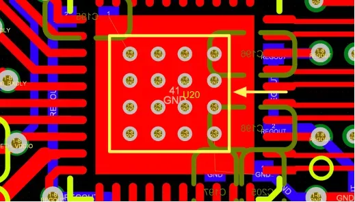
Copper layer files answer the question of where conductive features are kept. Soldermask layers describe openings in the soldermask material — they are not additional copper. Silkscreen carries text and identification information and cannot replace electrical connections. Although the design environment displays these items overlaid, outputs must make clear each file’s purpose to manufacturing.
Drill files answer where holes are located, their diameters, and related hole types and layer span (plated-through vs non-plated). Board-outline files must specify the final shape. Visual cues that look like holes or boundaries in the CAD view are not guaranteed to be correctly exported as manufacturing data. Deliver files in formats your supplier supports, and ensure attributes such as metallized vs non-metallized holes are unambiguous.
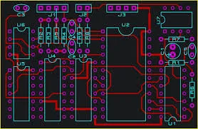
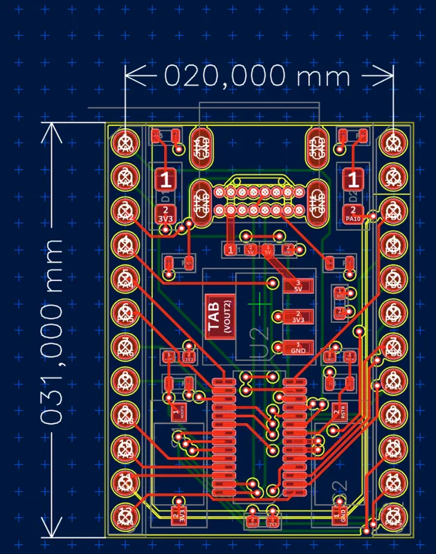
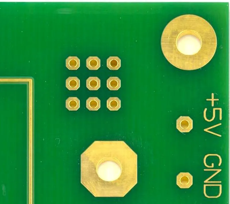
Figure 2 is a complete design view with various colored graphics and dimensions; Figure 3 shows the physical bare board. When comparing them, you don't need to study the circuit function — ask which design objects will become which physical features. This helps newcomers understand why sending a single overview image is insufficient.
Beyond Artwork: Put Requirements in One Specification
Board material, finished thickness, copper weight, surface finish, soldermask color — none of these should be left to guesswork. For multilayer boards, provide the stackup and related requirements. If you need controlled impedance, confirm with the fabricator which stackup will be used and what verification they require; if there is no impedance requirement, do not fill in a set of uncalculated, unverified numbers just to appear "professional."
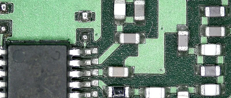
In Figure 4, the solderable area and surrounding soldermask-covered area are clearly distinct. Photos can help identify objects for the fabricator but cannot prove a particular thickness, copper weight, or process class. Likewise, screen colors and visual impressions cannot substitute for parameter specifications — write down important requirements and ensure they match the order options.
For a first submission, prepare a one-page checklist: project name, board number, revision, delivery scope, file purpose, key manufacturing requirements, and items pending confirmation. The format can follow your partner's template or use a structured manufacturing-information file both parties support. The point is not complexity of form, but avoiding three different answers for the same parameter in chat, the order, and the drawings.
Before Sending, Open the Package the Recipient Will Use
Do not rely solely on the CAD tool's "export successful" message. Place the archive you plan to send in a separate location, unzip it, and inspect it with a viewer that supports the chosen formats: are any layers missing, is the board outline clear, are copper layers aligned with the drill file, and do soldermask and silkscreen correspond? The object of inspection must be the final package to be sent, not the still-editing project in your design tool.
Also verify versions. After modifying the PCB, regenerate all affected manufacturing outputs — don't update only one file. Do not hand the fabricator several similarly named files like "final," "final_revised," and "really_final" and expect them to choose correctly. Keep a single clear release record that ties the file package to a design revision; subsequent changes generate new versions.
Finally, confirm the recipient can open the files and close any questions before production starts. It is not a substitute for professional design and manufacturing review, but it helps move from "I finished the design" to "someone can manufacture from these files."
Sending board files is not merely transmitting files — it is conveying the manufacturing intent clearly. Before placing the next order, open the final archive independently, cross-check the file list, versions, and order requirements; if any layer or parameter cannot be clearly attributed, resolve it rather than leaving assumptions for the production floor. Which requirement in your current fabrication package still exists only in chat and has not been entered into the formal documentation?