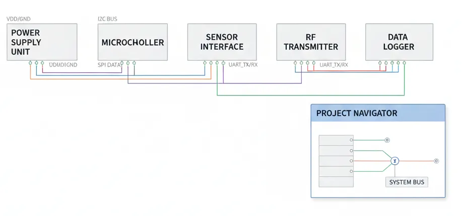
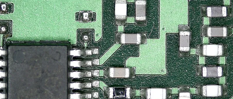
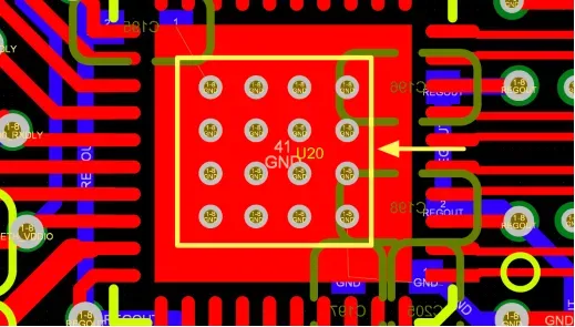
In electronic design, many persistent issues—signal interference, ADC conversion errors, unstable power rails, and EMI failures—ultimately trace back to how "ground" is engineered. Ground is not a mysterious link to the earth; it is the return-current path and the reference potential for every signal in the system. In complex designs, the way ground is planned and implemented directly determines signal integrity, electromagnetic compatibility, and overall system stability.
What Is "Ground" in a Circuit?
Ground (GND) is the return path for current and the common reference potential against which signals and supplies are measured. The ground network sets the stage for loop areas, parasitic inductance, and common impedance coupling. Poor ground architecture forces return currents to take long or discontinuous routes, increases loop inductance, encourages radiation, and injects noise into sensitive nodes. Good ground design provides continuous, low-impedance return paths, minimizes current loops, and confines electromagnetic fields.
Power Ground vs. Signal Ground
Power ground and signal ground serve different functions and carry different current profiles.
Power ground: Carries large currents and serves as the return path for power converters and loads.
Signal ground: Carries smaller currents as the return path for control, data, and mixed-signal nets.
Key design points for power and signal return paths include:
- Connect power input and output grounds to the nearest ground plane to minimize loop area and series inductance.
- Place decoupling and bulk capacitors close to device power pins to shorten the return path and close local high-frequency loops.
- Avoid return paths that detour across distant bypass capacitors. Long detours increase loop area and inductance, allowing di/dt noise to couple into other circuits and elevating EMI.
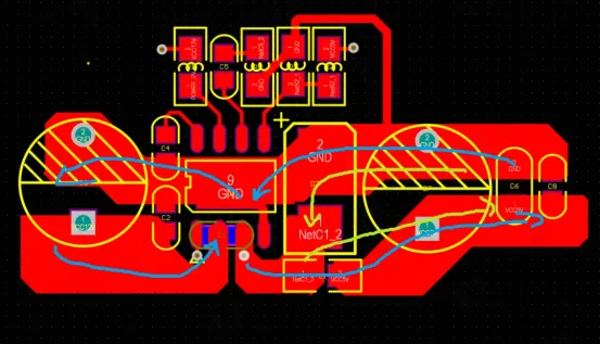
Figure 1 | Conceptual illustration of power return-path design
Return Paths Differ for Low and High Frequency
Return-current behavior depends on frequency because different impedance components dominate at different frequencies:
- Low-frequency signals (below approximately 50 kHz): Return current tends to follow the path of minimum resistance, which can be a broader route across copper if resistance is lower.
- High-frequency signals (above approximately 10 MHz): Return current minimizes inductive reactance and tightly follows the path directly under the signal trace when a solid ground reference is present. This requires tight coupling between the trace and its ground reference plane. Any gaps or splits in the reference plane force the return path to detour, substantially increasing loop inductance, degrading signal integrity, and increasing radiation.
For high-speed or high-frequency nets, ensure a continuous, closely coupled ground reference under the trace and use guard techniques to keep the return path short and local.
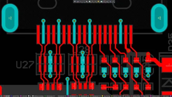
Figure 2 | Example of ground guarding around a high-frequency signal
Practical Ground Shielding Tips
- Stitch ground vias along both sides of critical traces to create a "via fence."
- Keep the return current close and "wrap" it around the signal path by maintaining a continuous ground reference and short stitching intervals.
- Confining electromagnetic fields improves signal integrity and reduces crosstalk to adjacent nets.
Keep Analog Ground and Digital Ground Separate
Analog ground (AGND) provides the reference for ADCs, DACs, op-amps, and other analog circuits. These nodes are highly sensitive to noise. Digital ground (DGND) serves high-speed switching devices such as MCUs and FPGAs, where return currents are rich in high-frequency content and can produce significant ground noise.
Mixing AGND and DGND indiscriminately allows digital switching noise to flow through the analog reference path. The result can be severe measurement error—for example, ADC outputs that look random under dynamic digital load conditions. To avoid this, partition analog and digital grounds by function and floor-plan the PCB so sensitive circuits remain isolated from high-noise blocks, with controlled paths for any necessary connections.
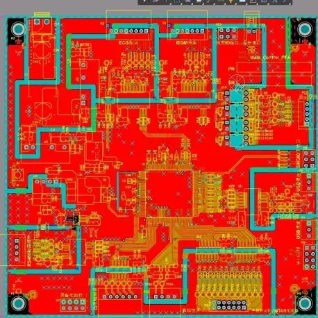
Figure 3 | Example of analog and digital ground region partitioning
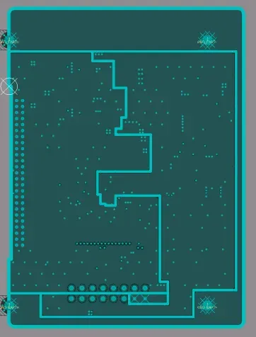
Figure 4 | Suggested spacing between ground regions (≥ 1 mm)
Layout Guidelines for Ground Partitioning
- Partition grounds by function (analog, digital, power) and organize the layout so signals and returns remain within their regions.
- Maintain ground-segmentation keep-outs and do not route across ground splits or slots. A split forces the return current to detour, increasing loop area and coupling noise into other circuits.
- Avoid routing power or sensitive nets across ground gaps. When a crossing is unavoidable, redesign the stack-up or region boundaries to provide a continuous reference plane.
Guard Ground: A Shield for High-Speed Signals
Guarding high-speed traces with ground is an effective way to confine fields and control return currents. For differential pairs and fast single-ended lines, place ground-via fences on both sides of the routing. This creates a tightly coupled trace-to-ground structure and closes the return path locally, enhancing signal integrity and reducing crosstalk. The approach is applicable to high-speed interfaces such as DDR, HDMI, LVDS, and USB when applied appropriately to the geometry and stack-up.
Figure 2 (repeated) | Ground guarding with via stitching for high-speed routing
- Use ground-via stitching along both sides of critical traces to form a "fence."
- The resulting closely coupled structure closes the return current loop and supports controlled impedance routing.
- Appropriate for DDR/HDMI/LVDS/USB and other high-speed interconnects when implemented with the correct spacing and stack-up.
Single-Point Grounding: Bringing It All Together
Regardless of how many ground regions you partition, the system must share a common reference. Ultimately, all ground regions should be connected at a deliberate, single point to control where noise flows and to prevent undefined ground potential differences.
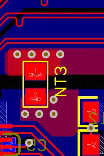
Figure 5 | Series single-point grounding topology
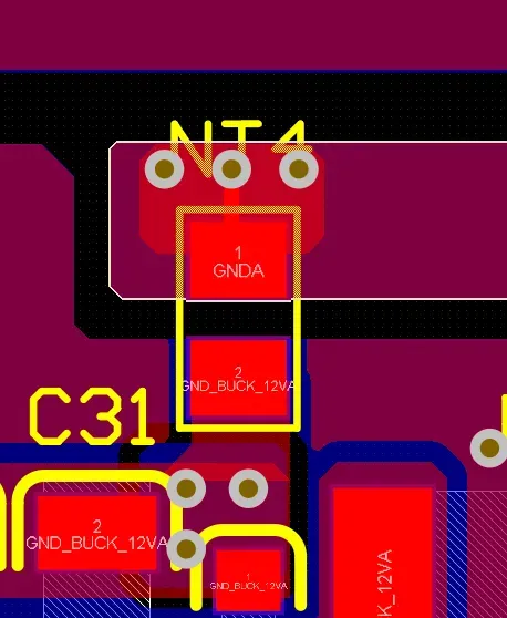
Figure 6 | Parallel (star) single-point grounding topology
Common approaches include:
- Series single-point connection: Simple, but segments share common impedance, increasing the risk of noise coupling between regions.
- Parallel (star) single-point connection: Stronger isolation because each region returns to the star point with its own path. It reduces common-impedance coupling but requires more routing resources and space.
A practical and tunable method is to connect partitions at a single point using a ferrite bead or a 0 Ω resistor. This allows attenuation of high-frequency noise, simplifies debugging, and provides flexibility to evaluate different grounding strategies during bring-up. Avoid multiple parallel ground connections that bypass the intended single-point path.
Summary Table
| Type | Application | Design Focus |
|---|---|---|
| Power ground | DC-DC, LDO | Shortest return path, close to high-current components |
| Signal ground | Control, data transmission | Guarding/ground shielding, tightly coupled to a GND plane |
| Analog ground | Op-amps, ADC | Keep away from digital noise, independent partitioning |
| Digital ground | MCU, FPGA | Large ground reference area, strong coupling to device ground pins |
| Guard ground | High-speed digital signals | Via fences along trace edges, close the return-current path |
| Partitioned ground | Mixed-signal systems | Maintain a single reference plane within regions, do not route across splits |
| Single-point ground | Multi-region systems | Use ferrite bead/0 Ω link at one point; avoid multi-point ties |
Checklist for a Robust Ground Implementation
- Does each signal have a short, continuous return path tightly coupled to its reference?
- Have you avoided routing across splits or slots in the ground plane?
- Are analog and digital grounds connected at exactly one deliberate point?
- Have you applied ground guarding to critical high-speed traces?
Addressing these questions early in layout prevents hidden ground-related problems from undermining system performance and compliance.