This article explains how to design PCB castellated holes in KiCad, how to configure design rules so DRC passes cleanly, and what to pay attention to during manufacturing.
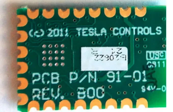
Figure 1 | Castellated hole concept
What Are Castellated Holes?
Castellated holes are a row of plated through-holes drilled along the edge of a PCB and then partially routed off during board profiling, leaving a half-hole at the board edge with exposed copper plating. This produces a scalloped, plated edge that allows the board to be soldered down like an SMD device while maintaining plated-through connectivity to internal layers.
Common English terms include:
- Castellation
- Castellated hole
- Plated half-holes
- Semi-plated holes
Module-style PCBs frequently use castellated edges to make assembly easier. Modules are small yet functionally dense, so designers place a row of through-holes right at the outer edge; during the final routing step, the profiling tool removes half of each plated hole, leaving a "half-hole" in the finished panel. This creates SMD-like edge pads that can be soldered onto a host PCB while providing robust metallurgical bonds.
Typical examples include ESP32-WROOM modules and the Raspberry Pi Pico microcontroller board, both of which mount using castellated edges.
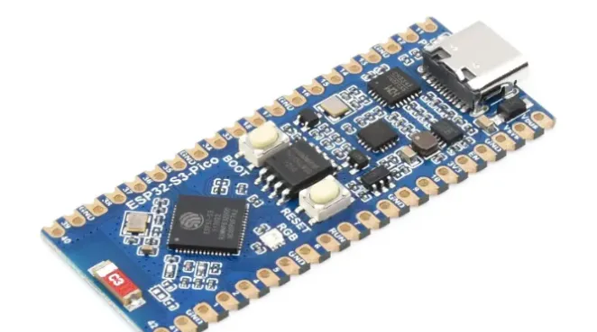
Figure 2 | Example of an SMD module with castellated holes for edge soldering
Implementing Castellated Holes in KiCad
Fundamentally, a castellated connection is just a plated through-hole (PTH) pad placed directly on the board edge. The pad is positioned so that the board outline passes through the center of the plated hole. After drilling and plating, the board is routed, and the profiling tool removes half of the hole, exposing the plated cross-section at the edge.
Viewed in KiCad's 2D and 3D modes, castellated half-holes look like standard PTH pads that intersect the board's Edge.Cuts outline.
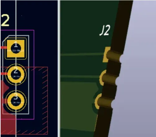
Figure 3 | Castellated pads in KiCad 2D/3D views
DRC Behavior in Earlier KiCad Versions
In versions prior to KiCad 7, placing a PTH pad on the Edge.Cuts outline typically triggered board-edge clearance violations. Because the pad's copper and hole overlapped the outline, the DRC engine treated it as a rule violation, and routing to or from the half-hole could be blocked.
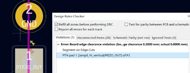
Figure 4 | DRC reports a board-edge clearance violation for on-edge PTH pads
In addition, routing from the board edge into the castellated pad was restricted by DRC, making it difficult to connect traces to these pads from the edge direction.
Even when routing from inside the board, the trace might fail to be recognized as connected to the pad's center because the pad geometry is split by the outline.

Figure 5 | The trace is not recognized as connected to the pad center
KiCad 7 and Later: Castellated Pad Attribute
Starting with KiCad 7, castellated holes are natively supported. In the pad's properties, under Manufacturing Attributes, set the attribute to "Castellated (THT only)". This informs the DRC engine that the pad intentionally intersects the board outline and should be treated as a castellated half-hole.
Once this attribute is applied, DRC properly recognizes castellated geometry. Clearance violations at the board edge are no longer reported for those pads, and routing to and from the pad works as expected.

Figure 6 | With the castellated attribute set, DRC passes and routing is normal
Practical KiCad Tips
- Create a dedicated footprint for castellated pads. Define PTH pads whose centers lie exactly on the intended board outline. Align the pad centers and the Edge.Cuts line so the outline bisects the holes.
- Use through-hole pads only. Castellated pads are plated holes that are later routed; they are not SMD-only features. Ensure the drill and annular ring meet your manufacturer's capabilities.
- Maintain consistent pitch and alignment. For modules intended to be soldered like SMD components, consistent spacing ensures predictable solder fillets and easy alignment during assembly.
- Set the pad's Manufacturing Attribute to Castellated (THT only) so DRC understands the geometry and allows proper routing and connectivity checks.
- Represent the board outline accurately. The final profiling toolpath follows Edge.Cuts. Make sure the outline passes through pad centers as intended.
Manufacturing Considerations
Castellated holes require extra process steps and tighter mechanical control, so they are significantly more expensive than equivalent PCBs without castellations. As a rough order-of-magnitude, costs can be several times higher. For low-cost prototypes, an alternative is to place a "sacrificial" perimeter and manually cut the board edge to expose half-holes, but expect lower quality and risk of damage; this is generally acceptable only for quick, disposable prototypes.
Why Castellated Holes Cost More
Castellated edges combine plated-through holes with routed edges that cut through those holes. This requires:
- Precise drill-to-route registration so the outline tool passes exactly through hole centers.
- Reliable copper plating of through-holes before routing, followed by clean edge routing that exposes a smooth, continuous plated cross-section.
- Additional inspection and potential deburring to remove burrs or "tear-out" at the plated edge cut.
- Potential yield loss if the routed edge damages the plated barrel or if the copper delaminates at the edge.
These steps add time and risk compared to standard boards, increasing cost.
Coordinate with Your PCB Manufacturer
Always confirm the manufacturer's capabilities and requirements for castellated features. Do not rely on generic "rules of thumb." Different fabricators may have different constraints on minimum drill size, annular ring width, copper-to-edge clearances, solder mask relief, and routing tolerances specific to castellated edges. Early communication avoids redesign and reduces risk of scrap.
Design Guidelines for Robust Castellations
- Hole size and annular ring: Choose a drill diameter and copper annulus that your fab can reliably plate and that will still provide adequate copper continuity after half the hole is removed. Avoid pushing absolute minimums unless the fab approves them.
- Copper-to-edge clearance: Ensure that adjacent copper features, planes, or pours maintain the fab's minimum distance from the castellated edge after routing to prevent exposed copper slivers and shorting risk.
- Routing tolerance and pad alignment: The board outline should pass through the pad centers. Provide adequate pad width and copper so minor routing tolerances do not leave a thin or discontinuous plated edge.
- Solder mask openings: Define mask openings that match your assembly method. Some designers prefer mask-defined edges to control solder spread; others allow larger openings for better wetting. Discuss with your assembler.
- Keep neighboring vias back: Avoid via-in-pad or close vias near castellated pads to reduce solder wicking and prevent weakening of the edge during routing.
- Panelization and support: Castellated edges remove copper and laminate along the perimeter, potentially weakening the panel edge. Use tabs or rails to support the board during fabrication and routing; consult the fab's panelization guidelines.
- Avoid sharp interior corners: Where castellations turn a corner (e.g., on L-shaped modules), maintain smooth outline transitions to reduce mechanical stress concentration at the plated edge.
Assembly and Soldering Notes
- Reflow vs. hand soldering: Castellated modules can be assembled by reflow or hand solder. For reflow, ensure paste apertures on the host PCB are tuned to produce solid fillets at the edge without excessive bridging. For hand solder, provide enough pad length on the host board to allow iron access and solder fillet formation.
- Mechanical stability: Castellated joints act like SMD leads. If the module is heavy or subject to vibration, consider additional mechanical features (e.g., mounting holes, adhesive) to offload stress from the solder joints.
- Inspection: The exposed plated cross-section at the edge makes visual inspection easier. Verify continuous copper plating across the edge and consistent solder fillets along the length of the castellation.
Troubleshooting Common Issues
- DRC still flags edge violations: Confirm the pad attribute is set to Castellated (THT only) and that the pad type is through-hole. Check your board outline layer and ensure the Edge.Cuts line accurately bisects the pad center.
- Net connectivity errors: If traces are not recognized as connected, verify the pad's net assignment and that the 3D/2D model aligns with the pad's actual position. Minor misalignment between pad center and outline can cause the connectivity engine to misinterpret geometry.
- Manufacturing feedback about tear-out: Increase annular ring, adjust hole size, or relax copper-to-edge spacing per fab guidance. Small geometry changes often resolve edge plating integrity issues.
- Solder bridging during assembly: Reduce paste aperture size on the host board, increase solder mask dams if allowed, or adjust the module's pad spacing if feasible.
Summary
Castellated holes enable small PCBs and modules to be soldered directly onto host boards as if they were SMD components, while preserving robust plated-through connectivity. In KiCad, implement castellations by placing PTH pads on the board edge and, in KiCad 7 and later, setting the pad Manufacturing Attribute to Castellated (THT only). This ensures DRC understands the on-edge geometry and allows normal routing and connectivity checks.
Because castellations drive tighter fabrication tolerances and additional processing, coordinate early with your PCB manufacturer and follow their specific capability limits. With proper pad geometry, accurate board outlines, and careful assembly planning, castellated modules can deliver reliable, compact interconnects with zero DRC violations and predictable manufacturability.