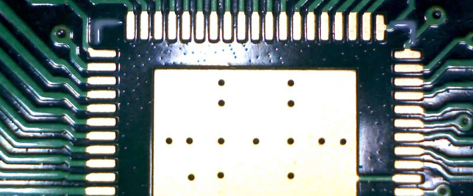
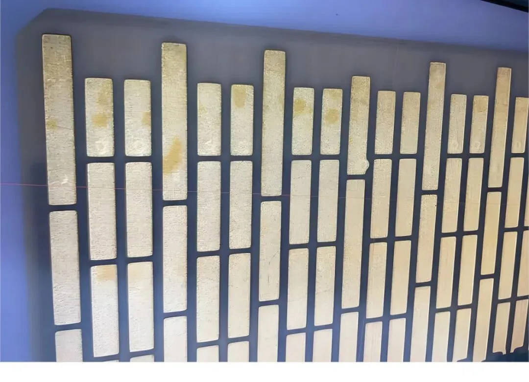
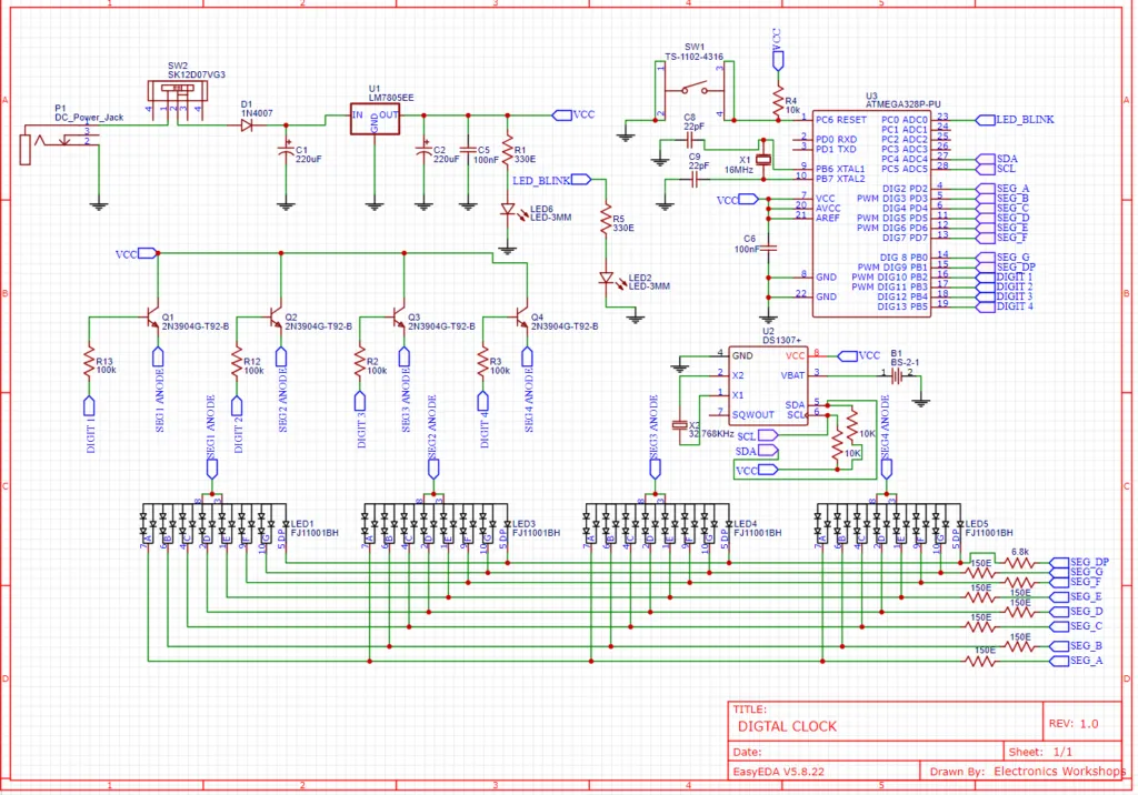
New energy, industrial automation, electric vehicles, and energy storage are raising power density, conversion efficiency, and reliability at the same time. Devices such as SiC and GaN bring faster switching, and they also make dv/dt, di/dt, parasitics, and EMI harder to control. What often separates a working design from a fragile one is not whether a board can be routed, but whether the power loops, safety spacing, thermal design, EMC, and production requirements can all be placed on the same board.
A correct schematic does not mean the board will be stable at power-up. A fully connected netlist does not mean the design will pass safety, temperature-rise, and EMC requirements.
01 | The Highest Cost on a High-Power Board Is Not Copper Foil
Routing experience from ordinary PCBs or high-speed PCBs cannot be copied directly into high-power work. A small miss in loop area, spacing, or heat spreading can become a burned board, oscillation, false triggering, excess temperature rise, or a failed certification at prototype and production.
- Current carrying is not "just make the trace wider." It must be judged with copper thickness, temperature rise, ambient temperature, via count, and the current loop.
- Safety spacing is not "open the gap by feel." Clearance and creepage are constrained by working voltage, pollution degree, CTI, and related conditions.
- A high-dv/dt node is not "fine as long as it can be routed." The area, placement, and coupling of the switching node and the high-di/dt loop directly affect ringing and EMI.
- A sensitive signal is not "better if it is shortest." Sampling, feedback, gate-drive, and control lines must also stay away from noise sources, and the split and connection of ground must be handled correctly.
02 | High-Power Layout Needs a System Capability Map
Layer 1: Read the topology and the energy flow
From flyback, buck/boost, PFC, and LLC half-bridge/full-bridge to boost plus full-bridge inversion, identify the power path and the switching states first.
Layer 2: Capture the critical loops and noise sources
Identify high-dv/dt nodes and high-di/dt loops. Control loop area, parasitics, and ground bounce first.
Layer 3: Calculate current carrying, thermal design, and safety spacing
Evaluate copper current-carrying capacity in the spirit of IPC-2152, plan vias and heat paths, and check safety spacing against the applicable conditions.
Layer 4: Close EMC, DFM, and delivery
Reduce EMI risk at the source, then complete DRC, safety checks, silkscreen, Gerber and production-file output, and a project review.
The core of this path is not memorizing rules. It is learning how, on a new power project, to derive layout constraints from the topology, then use a checklist and verification thinking to reduce trial and error.
03 | Six Power Levels, Six Sets of Constraints
The cases step from 20 W toward the kilowatt class. Each rise in power recombines the constraints of current, voltage, heat, safety, stackup, and EMC. Six projects correspond to six upgrades in engineering constraints.
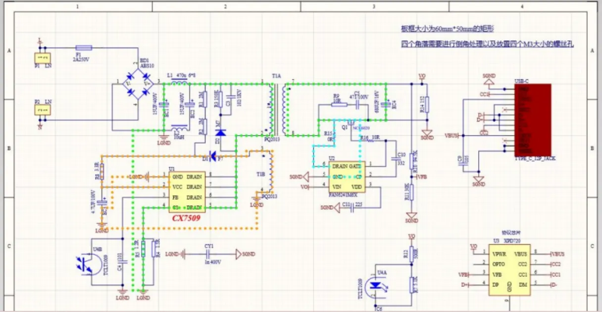
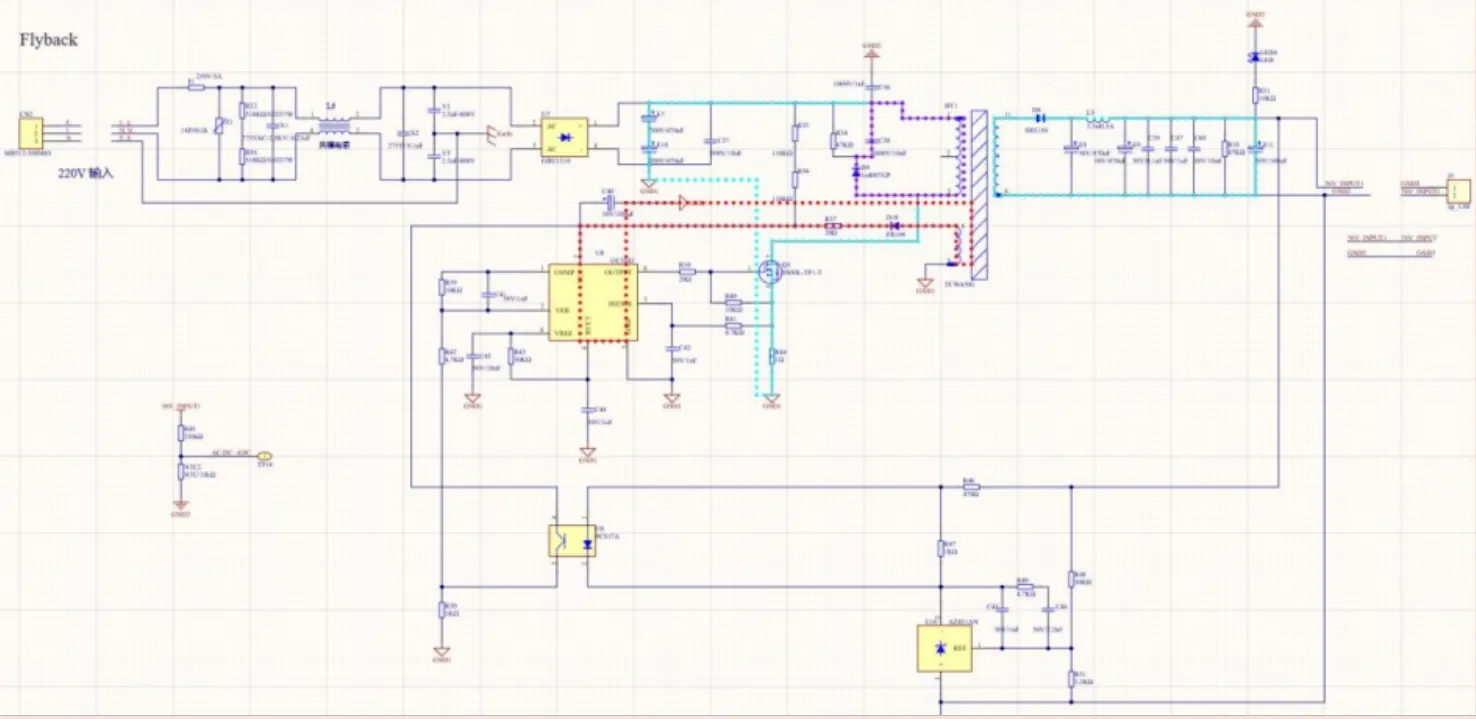
LEVEL 01 / 20 W — PD fast charge: flyback, safety, and the PD interface
Focus on the flyback primary, high-frequency transformer, synchronous rectification, and PD protocol control. Practice the critical loops, safety lookup, DFM/EMI details, and Gerber output.
Topics: flyback, IEC 62368, EN 55032-B, DFM.
LEVEL 02 / 90 W — Digital buck: wide-range voltage, high current, and mixed control and power design
Based on the GD32E51x MCU family, targeting 200 kHz, 0-30 V output, and 0-3 A adjustment. Practice ground splitting, critical loops, sensitive signals, and a two-layer control-board design.
Topics: buck, GD32, sensitive signals, split grounds.
LEVEL 03 / 460 W — Interleaved CRM PFC + LLC: multiple topologies, a multilayer board, and 40 A synchronous rectification
From EMI filtering, interleaved PFC, and an LLC half-bridge to analog/digital and multi-ground partitioning. Practice inner- and outer-layer high-voltage/low-voltage planning, copper and via current-carrying evaluation, and heat spreading in the power region.
Topics: interleaved PFC, LLC half-bridge, 40 A synchronous rectification, four-layer board.
LEVEL 04 / 500 W — Digital PFC + LLC: power board, control board, and multi-board interconnect as one system
Around a digital PFC + LLC half-bridge supply, analyze voltage/current sampling, OCP/OVP, MOSFET drive, primary/secondary handling, multi-board interconnect, and mechanical conflict review.
Topics: PFC + LLC, OCP/OVP, multi-board interconnect, mechanical review.
LEVEL 05 / 3500 W — DC charging: totem-pole PFC, LLC full-bridge, and kilowatt-class high-voltage/low-voltage design
Based on GD32G553 and a totem-pole PFC + full-bridge LLC scheme, targeting a 220 V input and 250-450 VDC output. Train control-circuit design, high-voltage/low-voltage partitioning, and the power path.
Topics: totem-pole PFC, LLC full-bridge, 3.5 kW DC charging.
LEVEL 06 / 3 kW — PV inversion: from boost to single-phase full-bridge
The main line is a two-stage non-isolated boost plus single-phase full-bridge VSI. Practice complex project floorplanning, heat-path evaluation, current-carrying and via calculation, high-voltage/low-voltage design, DFM checks, and project review.
Topics: boost, full-bridge VSI, heat path, DFM.
04 | A Question That Tests Whether the Method Holds
When a new project is placed in front of you, can you independently plan the stackup and partitioning, identify the critical power loops, calculate current carrying and vias, handle high-dv/dt nodes and sensitive sampling, and deliver the full flow of thermal design, EMC, safety, DFM/DFR, and production files?
From 20 W to 3.5 kW, every design rule has to become a delivery capability.