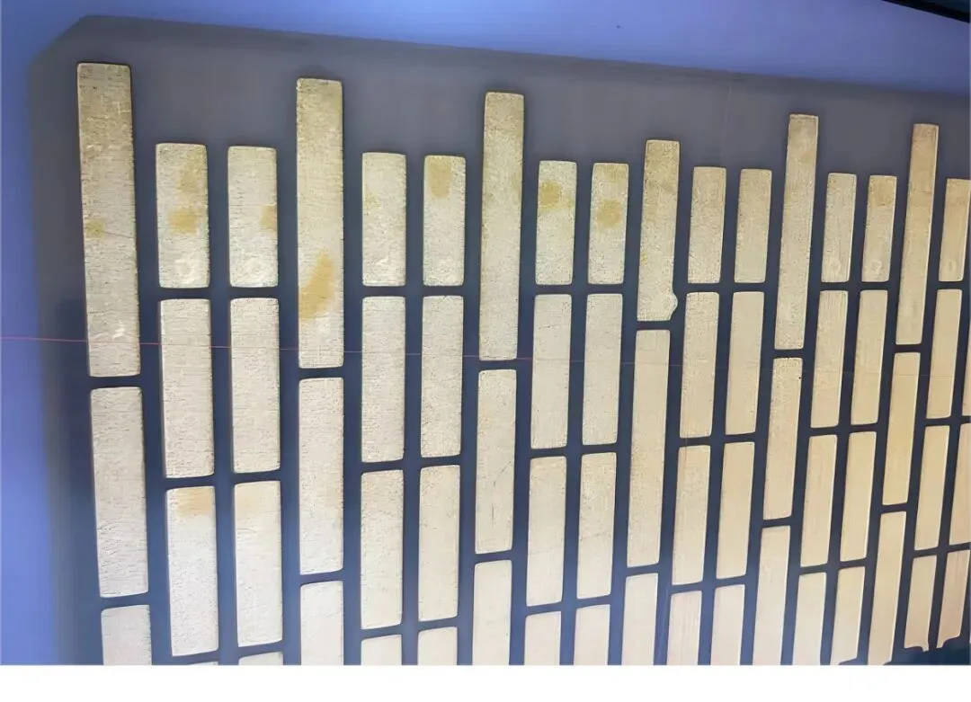
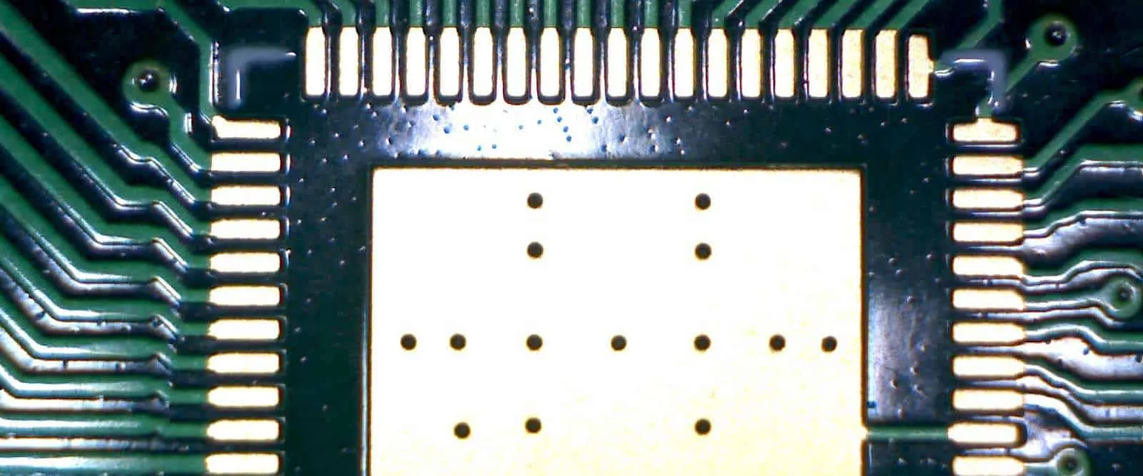
A solder mask bridge is the narrow strip of insulating solder mask that remains between adjacent pads or IC leads on a printed circuit board. Its primary function is to separate neighboring solderable areas and prevent molten solder from flowing between them during assembly. In practical terms, the solder mask bridge acts as a physical barrier that reduces the risk of solder bridging and unintended shorts.
Solder Mask Bridge Width Requirements
The achievable solder mask bridge width depends on the solder mask color, the exposure process, the board structure, and the manufacturing capability of the PCB fabricator. As a general manufacturing baseline, a green solder mask bridge is commonly designed at approximately 3 mil, while black solder mask may require approximately 5 mil. Other solder mask colors are often designed at approximately 4 mil.
These values represent practical dimensions that many conventional PCB production lines can manufacture with reasonable stability. When more advanced processes, such as laser direct imaging (LDI), are used, the minimum bridge width may be reduced to approximately 2 to 2.5 mil. However, the achievable value should be confirmed with the selected fabricator rather than treated as a universal design rule.

Key Factors That Determine Solder Mask Bridge Width
Pad-to-Pad Edge Spacing
The basic relationship between pad spacing, solder mask opening, and bridge width can be expressed as:
Solder mask bridge width = pad edge-to-edge spacing ? 2 × solder mask expansion on one side
For example, if the edge-to-edge spacing between two IC pads is 8 mil and the solder mask opening extends 2 mil beyond each pad edge, the remaining solder mask bridge is 4 mil:
8 mil ? 2 × 2 mil = 4 mil
This relationship shows why the bridge cannot be evaluated by looking only at the component pitch or pad size. The solder mask opening, also called solder mask expansion or swell, directly consumes the available space between adjacent pads. If the pad spacing becomes smaller or the opening becomes larger, the remaining bridge becomes narrower.
For the same reason, the design data should clearly define the intended solder mask openings. If the fabricator has to modify the openings to meet manufacturing rules, the resulting bridge width may differ from the original PCB layout.
Copper Thickness
Thicker copper generally requires a wider solder mask bridge. A thicker copper feature produces greater topography on the PCB surface, making it more difficult for the solder mask to cover narrow spaces consistently. The additional height can also make the mask more vulnerable to thinning or discontinuity around the edge of the copper feature.
As a practical reference, 1 oz copper is associated with a bridge-width baseline of approximately 3 mil in the described design context. For 2 to 4 oz copper, a bridge of at least approximately 3.5 to 4 mil may be required. These values are process-dependent, so the final design should be checked against the fabricator's capability for the actual copper thickness and solder mask process.
Solder Mask Color
Solder mask color also affects process capability. Green solder mask is generally the most mature and forgiving process. Other colors can have different optical properties, pigment distributions, and exposure behavior. Black solder mask is especially challenging for fine solder mask features because imaging and inspection conditions can be less favorable.
Therefore, a bridge width that is acceptable for green solder mask may not be equally reliable for black or other colored solder masks. When the design contains fine-pitch components, solder mask color should be treated as a manufacturing variable rather than as a purely cosmetic choice.
Recommended PCB Design Practices
Maintain Adequate Pad Spacing
When board space permits, an edge-to-edge spacing of at least 0.20 mm, or approximately 8 mil, between adjacent IC pads is recommended in the described design scenario. With a typical single-side solder mask opening of 2 mil, this spacing can provide a solder mask bridge of approximately 4 mil.
A similar minimum spacing can also be used as a reference for ordinary adjacent pads. Maintaining sufficient room between pads improves the probability that the bridge will remain continuous after solder mask imaging, development, and curing. It also gives the solder mask process more tolerance to registration variation.
When space is severely constrained, the solder mask expansion on each side may be reduced from the conventional 2 mil to approximately 1 mil, provided that solderability and assembly requirements remain satisfied. This approach increases the space available for the bridge, but it requires tighter process control and may depend on LDI exposure equipment. It should therefore be reviewed jointly by the PCB designer, assembler, and fabricator.
Consider the Assembly Process
The solder mask bridge is particularly important around fine-pitch ICs, where the distance between adjacent leads is small. During reflow soldering, solder paste melts and spreads across the pad surface. Surface tension and wetting behavior can help keep solder on the intended pads, but they cannot always compensate for insufficient separation or excessive paste volume.
A continuous solder mask bridge provides an additional physical boundary between neighboring pads. It does not replace correct stencil design, solder paste control, component placement accuracy, or reflow-profile control, but it reduces the sensitivity of the assembly process to these variables.
What Happens When No Solder Mask Bridge Is Used?
When the spacing is too small to maintain a reliable bridge, a fabricator may combine the solder mask openings of multiple adjacent pads. This condition is often described as a common opening or an opening without a solder mask bridge. The solder mask between the pads is removed, leaving one continuous exposed area.
A common opening significantly increases the risk of solder bridging between adjacent pads. Without the insulating barrier, molten solder can spread more easily from one pad to the next. The resulting short may be detected during inspection, but it can also create rework, yield, and reliability problems.
For this reason, a common opening is generally not preferred unless it is required by a special component or layout condition. If the design intentionally permits solder mask to be removed between adjacent pads, that condition should be clearly specified in the fabrication documentation. Otherwise, the fabricator may treat the region as a high-risk soldering area and may request clarification or a design change.
Core Functions of the Solder Mask Bridge
Physical Prevention of Solder Bridging
During reflow soldering, molten solder paste wets the exposed pad surfaces. The solder mask bridge separates neighboring pads and acts as a physical barrier that limits lateral solder flow. This reduces the chance that solder will connect adjacent IC leads and form an electrical short.
The bridge is therefore the first line of defense against solder bridging. However, the final result also depends on solder paste volume, stencil aperture design, pad geometry, component placement, and reflow conditions. A bridge improves the process margin, but it cannot eliminate every assembly defect by itself.
Protection of the PCB Surface
The solder mask also protects the material between adjacent copper features. Areas between pads may expose the FR-4 surface or other PCB dielectric material to contamination, moisture, flux residues, and thermal stress. Maintaining solder mask coverage helps isolate these regions from the assembly environment.
A continuous bridge can therefore provide more than pad separation. It also helps preserve surface insulation between adjacent conductors. If the mask is missing, damaged, or poorly registered, the exposed region may be more vulnerable to contamination and process-related degradation.
Control of Solder During Wave Soldering
In wave soldering, the PCB passes over a wave of molten solder. A solder mask bridge can help keep solder away from the spaces between closely positioned leads and can reduce solder climbing toward unwanted areas near the lead roots. It may also help reduce solder splashes and localized solder accumulation.
Although many fine-pitch ICs are assembled by reflow rather than wave soldering, mixed-technology boards may use multiple assembly processes. The bridge must therefore be evaluated in the context of the complete manufacturing flow rather than only one soldering operation.
Should a Solder Mask Bridge Always Be Included?
When the layout and manufacturing process can support a reliable bridge, retaining it is generally the safer choice. Removing the bridge transfers more responsibility to solder paste deposition, component placement, reflow control, and inspection. Small variations in any of these areas can then have a greater effect on the risk of solder bridging.
A bridge should not be forced beyond the fabricator's capability, however. If the required feature is narrower than the stable process limit, the bridge may become discontinuous, uneven, or absent after manufacturing. The correct approach is to balance pad spacing, solder mask expansion, copper thickness, mask color, exposure capability, and assembly requirements.
In short, a solder mask bridge is a small PCB feature with a significant manufacturing function. It separates adjacent pads, reduces solder-bridge risk, protects the surface between conductors, and improves assembly-process margin. Whenever the available spacing allows a stable bridge to be manufactured, including it is usually preferable to relying entirely on solder paste and reflow-process control.