An optical module is fundamentally a high-speed communications device that performs optical-to-electrical and electrical-to-optical conversion. A typical module integrates optical components, electronic ICs, a PCB, mechanical structures, and thermal-management components.
Key Characteristics of Optical Modules
High-Speed, High-Frequency Operation
Data rates have evolved from 1G and 10G to 25G, 100G, 200G, 400G, 800G, and beyond. As the data rate increases, signal integrity (SI), power integrity (PI), and high-speed interconnect design become increasingly demanding. The electrical interface must maintain controlled impedance and predictable signal behavior across the module, PCB, connector, and host equipment.
Combined Optical and Electrical Functions
An optical module contains both optical and electronic functions. Depending on the architecture, the device may include lasers or modulators, photodetectors, DSPs, CDRs, drivers, TIAs, and other high-speed components. As a result, its manufacturing and test processes involve both optical and electronic technologies.
High Density and Miniaturization
Common package formats include SFP, SFP28, QSFP, QSFP-DD, and OSFP. These packages integrate high-speed circuitry, optical components, mechanical structures, and thermal-management features within a limited volume. The available PCB area is therefore highly constrained, while routing, component placement, optical coupling, and mechanical alignment all need to be controlled simultaneously.
Sensitivity to Thermal Management
The power consumption of high-speed ICs and optoelectronic components increases as module performance advances. Heat-flow paths, thermal resistance, temperature rise, and component operating temperature therefore become important design factors. Thermal constraints can also interact with mechanical design and material selection.
High Reliability Requirements
Optical modules are commonly required to operate continuously in communications equipment. Reliability considerations may include temperature cycling, damp heat, mechanical stress, insertion and removal life, contact reliability, and high-speed electrical performance over the intended operating period.
Highly Standardized Interfaces
Mechanical dimensions, electrical interfaces, management interfaces, and optical interfaces are commonly constrained by MSA specifications, IEEE standards, OIF specifications, or related industry requirements. This gives optical-module design a strong emphasis on compatibility with standardized host systems and connectors.
However, optical modules with different data rates, package formats, and application conditions can differ substantially in chip composition, optical architecture, power consumption, and manufacturing complexity. The characteristics listed above should therefore not be treated as a fixed configuration for every optical module.
Why Are Optical-Module Gold Fingers Segmented?
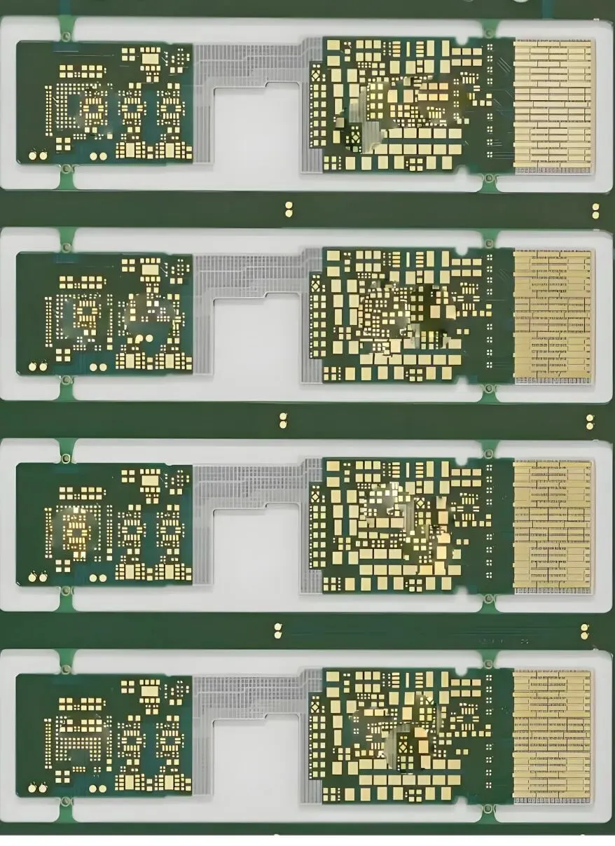
When an optical module is inserted into a switch, server, or other host device, the PCB edge normally contains plated contact areas commonly known as gold fingers. The term "segmented gold fingers" refers to the arrangement of these contacts into different functional regions. The purpose is not simply visual appearance. The contact areas are organized and separated according to their electrical functions and mechanical requirements.
Electrical Functional Separation
High-speed differential signals, power, ground, and low-speed control or management signals must be arranged according to the interface definition. The gold fingers consequently form different contact regions that correspond to these functions. This arrangement allows the module-to-host interface to follow the required pin assignment and electrical architecture.
Reduced Coupling Between High-Speed Signals
The arrangement of signal, ground, and power contacts affects the electromagnetic relationship between adjacent interface contacts. Proper placement of ground and power contacts can help control coupling and crosstalk between high-speed signals. It also supports a more predictable return-current path through the connector and host interface.
Improved Signal Integrity
A high-speed differential pair must maintain impedance continuity and an appropriate return path through the entire channel. The arrangement, dimensions, spacing, and transition geometry of the contact areas all influence the signal-integrity performance of the interface. An unsuitable contact layout can introduce discontinuities that contribute to reflection, crosstalk, insertion loss, or return loss.
For this reason, segmented gold fingers should be understood as one part of the complete high-speed channel rather than as an isolated PCB edge feature. The contact geometry, connector structure, PCB stackup, and internal routing must work together to maintain acceptable electrical behavior.
Controlled Insertion and Removal Sequencing
Some interfaces use contacts with different lengths to establish a defined connection sequence. Ground, power, and signal contacts can then be connected or disconnected in the required order during insertion and removal. This arrangement helps prevent undesirable electrical states while the module is only partially engaged with the host connector.
The segmentation and length differences therefore serve both functional and electrical purposes. They are related not only to pin grouping, but also to the way the interface behaves during the physical insertion process.
Improved Contact Reliability
Different contact regions may have requirements related to contact resistance, wear resistance, plating quality, and insertion life. The gold-finger structure and surface finish must therefore be compatible with the mating connector. Surface condition, coating uniformity, and mechanical geometry all affect the long-term reliability of the electrical connection.
A more accurate engineering interpretation is that segmented gold fingers use functional contact zoning, controlled geometry, and, where necessary, contact-length differences to satisfy high-speed electrical performance, power and ground return-current requirements, and insertion sequencing requirements at the same time.
Key Manufacturing Challenges of Segmented Gold Fingers
The main difficulty is not simply producing gold fingers. The challenge is converting the design requirements into stable mass-production capability under high-density, high-speed, and high-reliability conditions.
Dimensional and Positional Accuracy
Gold fingers involve multiple dimensional requirements, including width, spacing, length, chamfer geometry, edge position, and board thickness. Etching, plating, routing, profiling, and other PCB processes can each contribute to dimensional variation, resulting in accumulated tolerances.
For high-speed optical modules, positional deviation at the contacts can affect both connector mating and high-speed channel performance. Variations in contact geometry can also influence the physical engagement between the module and the host connector. Manufacturing control must therefore address not only whether the contacts are electrically connected, but also whether their dimensions remain within the required mechanical and electrical window.
Plating Quality and Insertion Life
Gold fingers generally require good wear resistance and stable contact performance. Manufacturing control therefore includes plating thickness, thickness uniformity, surface cleanliness, adhesion between the gold layer and its underlying metal, and visible defects such as scratches, pits, or exposed copper.
The change in contact resistance after repeated insertion and removal is also important. During volume production, the board-edge position, current distribution, and fixture contact conditions can affect plating uniformity. These factors may produce local variation even when the overall plating process appears to be correctly configured.
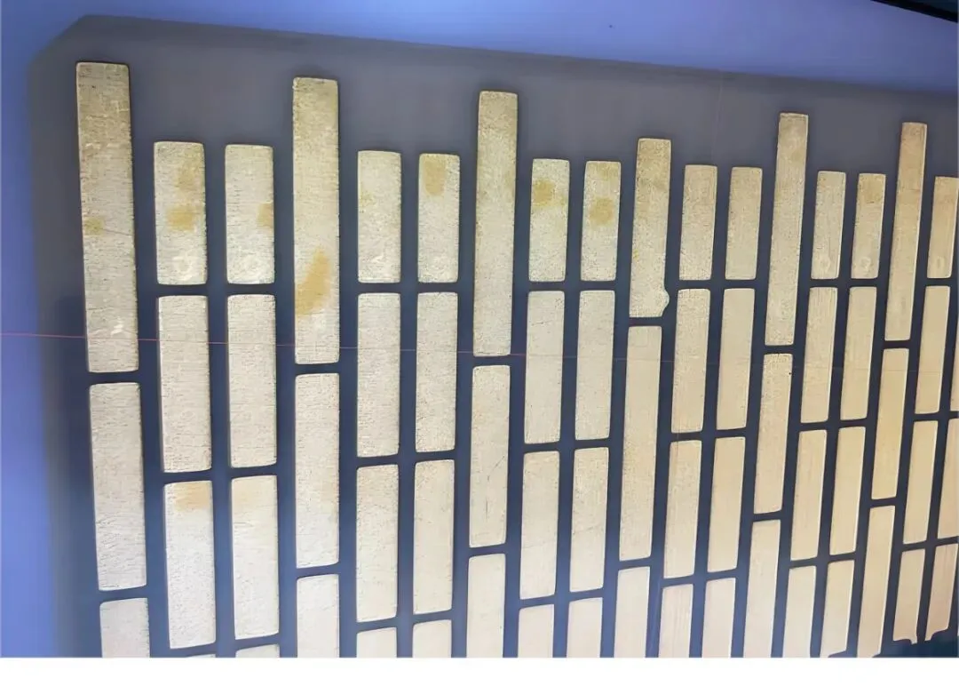
Process Window for Segmented Contact Regions
Segmented gold fingers often combine different contact lengths, multiple functional regions, and relatively small spacing. The manufacturing process must control pattern accuracy, plating uniformity, and final-form accuracy at the same time. The process window can therefore be more sensitive than that of a simple and uniform contact pattern.
Small deviations may affect several requirements simultaneously. For example, a positional error can influence connector mating, while a plating variation can affect contact reliability. The interaction between geometry, surface treatment, and mechanical forming makes process capability an important part of the design evaluation.
Consistency of High-Speed Electrical Performance
As optical modules progress into 100G, 400G, 800G, and higher-speed generations, PCB manufacturing cannot be evaluated only by whether the circuit is electrically continuous. Dielectric thickness, dielectric constant, copper thickness, trace width and spacing, and etch-related variation can all influence impedance, insertion loss, and return loss.
Manufacturing control must therefore be linked to the signal-integrity requirements of the design. PCB process variation can affect the electrical channel from the internal high-speed devices through the board traces and segmented edge contacts to the host connector. A module may pass a simple continuity check while still exhibiting unacceptable high-speed electrical variation.
Coordination of Multiple Materials and Processes
An optical module is rarely only a PCB manufacturing problem. It also involves optical-component attachment, chip placement and soldering, connectors, mechanical parts, and thermal materials. These materials can differ in coefficient of thermal expansion (CTE), thermal conductivity, and mechanical behavior.
After assembly, these differences may generate warpage, mechanical stress, or thermal-reliability problems. The PCB, optical components, connector, and heat-dissipation structure must therefore be considered as an integrated assembly rather than as independent elements.
High-Density Assembly and Yield
The product may be small, but its component density is high. SMT, precision placement, soldering, optical coupling, and electrical testing are closely interconnected. A small deviation in one process may not become visible until a later optical or high-speed electrical test.
Manufacturing yield, failure localization, and test coverage are therefore major concerns in volume production. Stable results require control across the complete process chain instead of relying on final inspection alone.
Engineering Summary
The central manufacturing challenge for an optical module is to maintain high-speed electrical performance, optical performance, thermal behavior, mechanical fit, and long-term reliability within a limited physical size. The design tolerances for all of these requirements must be converted into repeatable manufacturing capability.
Segmented gold fingers primarily support interface functional separation, high-speed signal integrity, power and ground return-current paths, and insertion sequencing. The manufacturing side must address dimensional accuracy, plating quality, insertion durability, impedance and loss control, and overall assembly yield. Their segmented appearance is therefore the visible result of coordinated electrical, mechanical, and manufacturing requirements at the optical-module interface.