










Double-sided adhesive tape on an FPC looks simple in the stack-up drawing. In practice it is one of the more frequent sources of assembly defects when the tape area is not designed with process limits in mind.
FPC adhesive tape design and flexible PCB double sided tape placement directly affect solder joint access, bond reliability, and cosmetic quality. Poorly defined tape regions create overflow, pressure marks, and blocked pads that only appear after lamination or final assembly.
Core Principles for Adhesive Tape Area Design
The tape exists to create a controlled bond between the flex and a stiffener, housing, or secondary surface. That bond must be strong enough for the application yet must not interfere with any electrical or mechanical function of the circuit.
Three principles govern the design. First, the tape must stay clear of every feature that needs to remain accessible or free of adhesive. Second, the tape outline must be sized so that adhesive does not flow beyond the intended zone under pressure and heat. Third, the pressure applied during bonding must not leave permanent marks on copper, coverlay, or components.
Ignoring any one of these principles produces defects that are expensive to rework once the tape is cured or the assembly is closed.
Why Tape Must Avoid Pads and Coverlay Openings
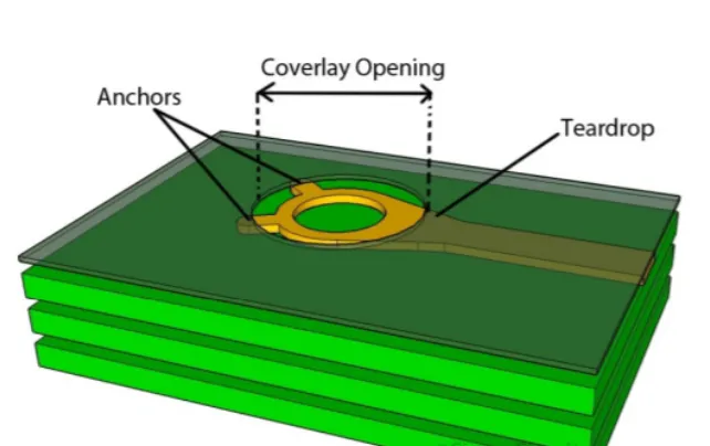
Solder pads, test points, and coverlay openings exist to provide electrical access. Adhesive on those surfaces blocks that access.
If tape covers even part of a pad, solder wetting is incomplete. The joint may pass continuity but fail mechanical testing. On fine-pitch components the risk of tombstoning or open joints rises. Gold fingers or connector contact areas that receive adhesive become unreliable contact surfaces.
Coverlay openings that are partially or fully taped over lose their purpose. Any copper that was intentionally exposed for soldering or probing is now masked. Removing the adhesive later usually damages the pad or the coverlay edge.
The keep-out is not optional. A practical minimum clearance from tape edge to any pad or opening is 0.5 mm. In high-density areas or when the adhesive is soft and high-flow, 0.8 mm to 1.0 mm provides safer margin. These distances account for both placement tolerance of the tape and any lateral flow during pressing.
Controlling the Actual Bonding Area of the Tape
The drawn tape outline is not the final bonded area. Under lamination pressure and temperature the adhesive softens and flows. The effective bond line expands beyond the original cut edge of the tape.
If the designer draws the tape exactly to the edge of a keep-out zone, the flowed adhesive will cross that zone. Pads that were nominally clear become contaminated. Coverlay openings that were safe become partially filled.
The amount of flow depends on adhesive type, thickness, temperature, pressure, and dwell time. Soft acrylic adhesives flow more than harder or thermosetting systems. Thicker tape generally produces more squeeze-out.
A reliable approach is to design the tape outline smaller than the maximum allowable bond area by the expected flow distance. For many common FPC double-sided tapes this means keeping the cut edge of the tape 0.3–0.5 mm inside the final permitted boundary. The fabricator or assembly house can confirm the actual flow behavior of the chosen tape.
Defining the tape as a strict keep-in region rather than a maximum region prevents the flow from becoming an uncontrolled variable.
Preventing Adhesive Overflow and Pressure Marks
Overflow and pressure marks are two related but distinct problems.
Overflow occurs when adhesive is squeezed outside the intended zone. It contaminates pads, bridges conductors, or creates cosmetic defects on the visible surface of the assembly. Once cured, the excess adhesive is difficult to remove without damaging the flex.
Pressure marks appear when the bonding pressure is transmitted through the tape into the copper or coverlay, leaving permanent indentations. These marks can thin the copper, create stress concentrations, or become visible cosmetic rejects. Components placed near the tape edge can also be damaged by uneven pressure.
Both issues are reduced by proper tape geometry and process control. Keep the tape away from high-relief features. Avoid placing tape directly under or immediately adjacent to thin copper traces that cannot tolerate compression. Use progressive pressure or compliant layers during bonding when the stack is sensitive.
On the design side, the most effective control is still geometric: give the adhesive room to flow without reaching critical features, and keep high-pressure zones away from delicate copper or components.
Practical Keep-Out and Coverage Rules
A working set of rules for most FPC adhesive tape applications includes the following.
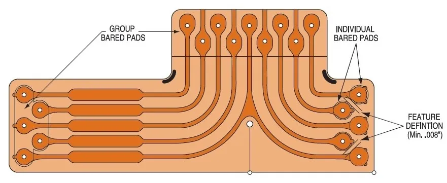
Maintain at least 0.5 mm clearance from tape edge to any solder pad, test point, or coverlay opening. Increase to 0.8–1.0 mm when the adhesive is known to be high-flow or when placement tolerance is large.
Keep tape clear of gold fingers, connector contact zones, and any area that must remain free for subsequent soldering or inspection.
In dynamic flex regions, evaluate whether the tape restricts the intended bending. Tape that crosses a high-flex zone can raise the neutral bend axis or create a stress concentration at the tape edge.
Define the tape outline as a closed shape with smooth corners. Sharp internal corners in the tape cut can tear during handling or create local pressure peaks.
When the tape is applied to only one side of a double-sided flex, confirm that the opposite side remains free of adhesive contamination from squeeze-through at vias or edges.
Document the tape material, thickness, and required bonding pressure in the fabrication or assembly notes. The design geometry alone does not fully define the process.
Common Design Mistakes That Surface at Assembly
Drawing the tape to the exact edge of a pad or opening is the most frequent error. It assumes zero placement tolerance and zero adhesive flow. Neither assumption holds.
Another common choice is covering large continuous areas without considering pressure distribution. Uniform pressure is difficult to achieve over large tape regions; local high-pressure spots produce marks while low-pressure spots produce weak bonds.
Designers also sometimes omit tape keep-out around stiffener edges or housing features that will later apply additional pressure. The combined stack then exceeds the compression limit of the copper or coverlay.
These mistakes are rarely visible in the CAD model. They appear only after the tape is applied and the assembly is inspected or tested.
Engineering Takeaway
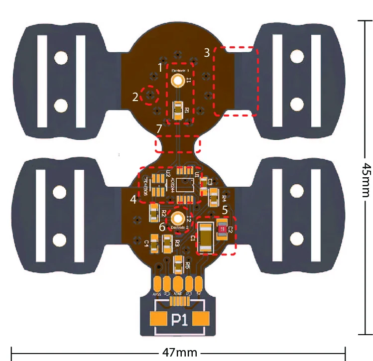
Reliable FPC adhesive tape design requires deliberate keep-outs around pads and openings, controlled coverage that anticipates adhesive flow, and geometry that avoids pressure marks. Flexible PCB double sided tape is not a free-form layer; it is a process-sensitive material that interacts with every nearby feature.
Define the tape area with clearance, flow allowance, and pressure distribution in mind. Those three considerations prevent the majority of tape-related assembly defects before the first part is bonded.






