The neck where a thin trace meets a pad is easily weakened by drill wander, process variation, and mechanical stress. A teardrop adds copper at that weak point. Applying teardrops to an entire board in one click can also suddenly widen a high-speed trace that was meant to stay uniform. A teardrop is both a mechanical and fabrication reinforcement and a new electrical structure. The question is not whether to add them. It is which nodes deserve them and which nodes must be treated with care.
What a Teardrop Reinforces
When a trace meets a round via pad directly, the copper narrows quickly near the tangent point. If the drill is offset from the pad, or etching thins the neck further, the remaining copper width can fall below the design value. A teardrop joins the pad and the trace with a tapered copper shape, raising tolerance to process error and reducing local stress through thermal cycles or flexing. That reinforcement has clear value on high-current nets, board-edge connections, connectors that see insertion force, and pads with a tight annular ring.
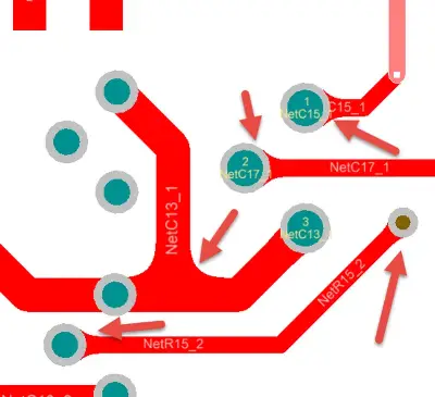
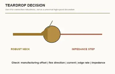
Wider Copper Is Also an Impedance Change
On slow-edge control nets, a local copper addition is often not the main concern. On high-speed single-ended or differential traces, a sudden widening raises local capacitance. A short transition then behaves like an impedance step. If the teardrops on the two sides of a differential pair differ in shape or in their relationship to the reference plane, asymmetry increases. The impact cannot be judged from frequency alone. Edge rate, geometry, and the total number of series discontinuities all matter. Dense BGA fanout is where small additions add up.
Do Not Cover the Whole Board With One Rule
A practical approach is to classify first. Power vias, ground vias, high-current pads, board-edge connectors, and mechanically loaded areas can use more aggressive teardrops based on the fabricator's drill wander and minimum remaining copper width. High-speed clocks, serial links, differential pairs, RF feed lines, and sensitive analog nodes should be grouped separately. First check whether the pad and trace already meet fabrication margin. When reinforcement is still needed, use a longer, symmetric taper to reduce the step. Do not rely on default parameters.
Answer High-Speed Nodes With Measurement
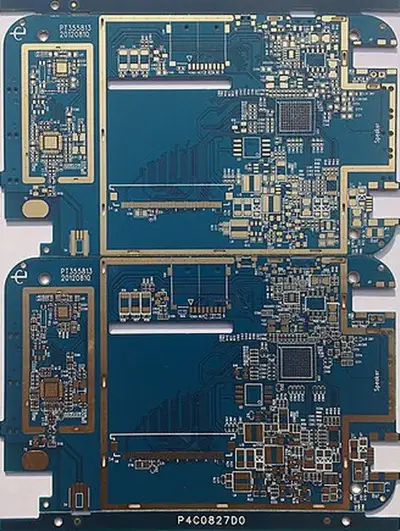
To judge whether a teardrop affects a link, start with cross-section geometry and a reflection estimate. Then compare impedance, return loss, and differential-to-common-mode conversion with and without teardrops using 2D or 3D electromagnetic tools. On a prototype, keep comparable via structures and observe the difference with TDR or eye diagrams under the same stimulus. If the difference is far smaller than other discontinuities and system margin, the fabrication benefit can stay. If the node is already on the edge, change the pad, trace width, or transition first.
Make Teardrops a Traceable Rule
A review should not stop at a report that says teardrops were added. Record the nets they apply to, the nets they exclude, shape, length, width, and when they are regenerated. After a via change, a width change, or a new fanout, old teardrops can remain, overlap, or lose symmetry. Regenerate them and run DRC on the finished copper. Before releasing fabrication data, check annular-ring margin, solder-mask openings, copper-to-drill clearance, and symmetry on both sides of each differential pair. The fabricator can then see the design intent, and a later tool or revision will not inherit history from one default option.
Also separate the connection goals of through-holes, blind vias, buried vias, and component pads. Microvias differ from mechanically drilled holes in copper thickness, pad diameter, and laser drill wander, and BGA fanout is limited by pitch. Enlarging a teardrop only to make the copper look thicker can squeeze adjacent channels, break differential-pair symmetry, or raise copper-to-copper spacing risk. On ordinary load pads, a teardrop does not replace correct trace width, thermal-relief settings, and current-carrying calculations. On RF and high-speed vias, a static impedance number is not enough; also check return vias, reference-plane changes, and via stubs.
When working with the fabricator, request drill-wander, minimum remaining copper width, and annular-ring capability, and put the real process window into the rules. First-article cross-sections can target the smallest annular rings and the densest fanout to confirm that the teardrop actually preserves the connection. If the process is already stable, keeping high-speed nodes geometrically simple is usually easier to analyze and reproduce. If process margin is tight, correct pad size and fabrication specs first, then decide whether a teardrop is required.
After a rule change, re-export the fabrication layers and inspect them in a production view. Dynamic teardrops shown in some EDA tools can differ from the final Gerber or ODB++ copper depending on version, settings, and object type. Review the released manufacturing data, not a checked box in the UI. In the design library, add notes and net classes to the teardrop rules so later designers know why a class was excluded, instead of regenerating teardrops across the whole board when they see an empty field. Design intent survives a change of owner, revision, or fabricator only when it is stored in rules and data. If routing edits require regeneration, put that step on the release checklist so the manufacturing package does not keep old copper shapes.
A teardrop is not a switch for prettier copper. It is a local feature with a mechanical benefit and an electrical cost. Classifying by node, setting parameters from process capability, and closing arguments with measurement is more reliable than adding teardrops everywhere or banning them everywhere.