Many PCB engineers start pulling traces as soon as the board is open. With no plan, nets are missed, paths detour, or signal integrity collapses, and the respin cycle begins.
PCB routing is closer to city traffic planning. Parts are buildings. Traces are roads. Random connections congest the board and create collisions. The notes below cover routing priority, crosstalk control, and the rules that usually decide whether the board works.
1. Route in Order. Do Not Fill the Board at Random
Do not flood the whole board first. The sequence matters.
Three priority rules
- Critical nets first. Power, small analog signals, high-speed signals, clocks, and sync signals must be routed first.
- Density first. Start in the device or region with the most connections and the tightest routing. Take the hard area first.
- Special treatment for critical signals. Keep clocks, high-frequency nets, and sensitive signals on a dedicated layer when possible, and keep loop area to a minimum. Add shielding or extra spacing when needed to hold signal quality.
- Impedance-controlled nets must stay on an impedance-controlled layer. Do not cross a split. A split creates an impedance step and strong reflection.
2. Crosstalk Control: The 3W Rule
Crosstalk is a common high-speed problem. Two traces that run parallel for too long couple into each other and produce bit errors, noise, and instability.
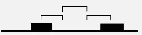
What the 3W rule is
Keep center-to-center spacing at least three times the trace width. That spacing is described as letting about 70% of the electric field stay from interfering with the neighbor, which is the usual statement of the 3W rule.
Three crosstalk controls
- Apply the 3W rule and increase spacing on long parallel runs.
- Insert a grounded isolation trace between sensitive nets.
- Reduce the distance from the routing layer to the ground plane so the return path is shorter and more stable.
3. Routing Rules That Can Fail a Production Board
These are baseline rules on production boards, high-speed boards, and high-frequency boards. Breaking them can drop performance, fail certification, or cause batch failures.
1. Adjacent layers must run orthogonal
- If the top layer runs horizontal, the next layer runs vertical.
- Do not run long parallel traces in the same direction on adjacent layers, or interlayer crosstalk rises sharply.
- If a high-speed board cannot avoid that, separate the layers with a ground plane and separate the signals with ground traces.
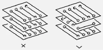
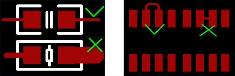
2. Small parts and fine-pitch pads need orderly exits
- Keep routing symmetric on small discrete parts.
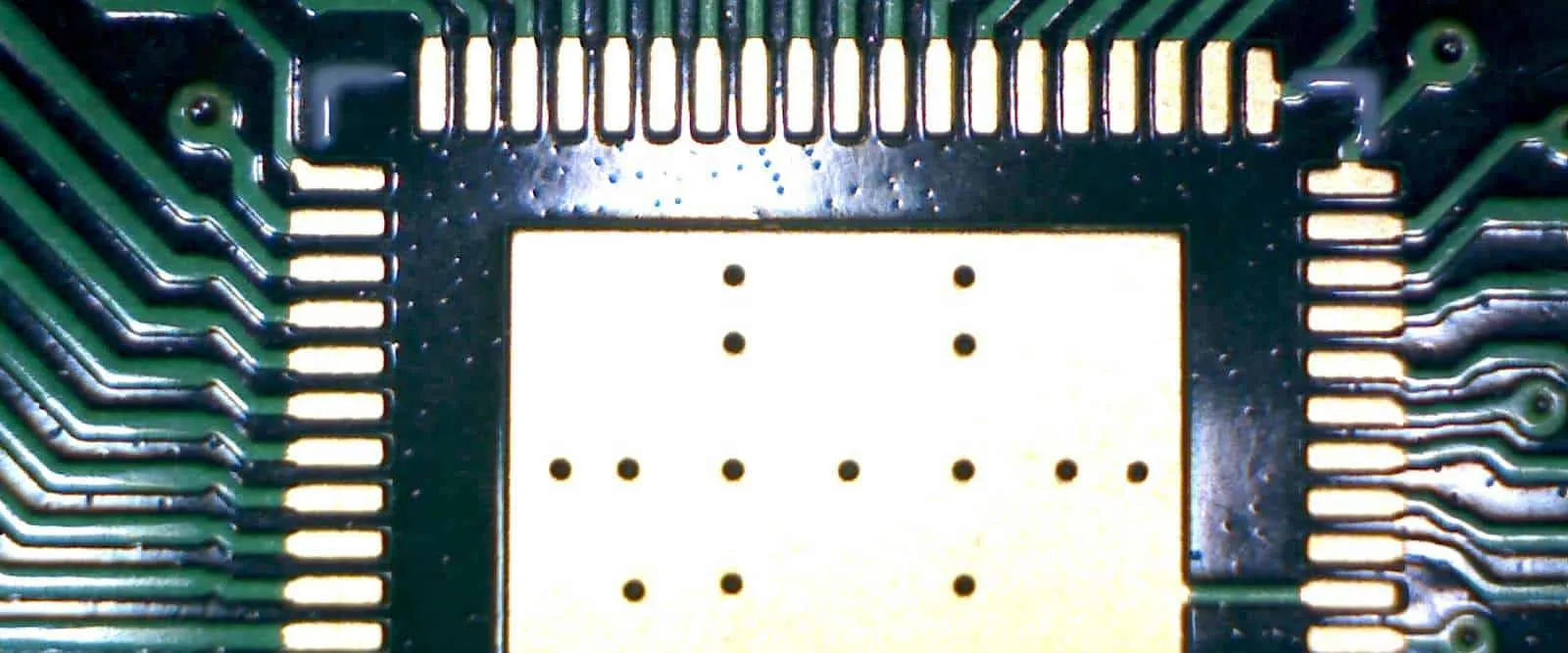
- On fine-pitch SMT pads, enter the pad from the outside. Do not run a trace through the middle of the pad.
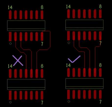
3. Keep the loop as small as possible
- The loop formed by a signal and its return should be as small as possible.
- A smaller loop radiates less and is more immune to interference.
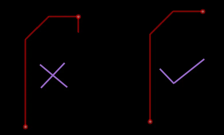
4. Do not leave stubs
On a high-speed net, a leftover stub causes reflection, ringing, and waveform distortion. Remove it.
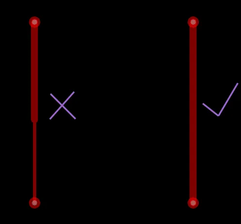
5. Keep width consistent on the same net
- A trace that changes from wide to narrow creates an impedance discontinuity and reflects a high-speed edge.
- If a width change cannot be avoided, such as at a BGA or connector, keep the transition as short as possible.
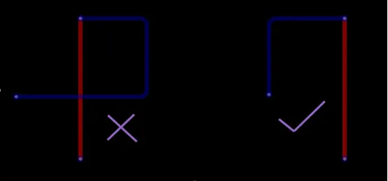
6. Do not create a cross-layer self-loop
- On a multilayer board a signal can be routed into a closed loop of its own.
- That self-loop acts as an antenna and radiates. Tear it up and reroute.
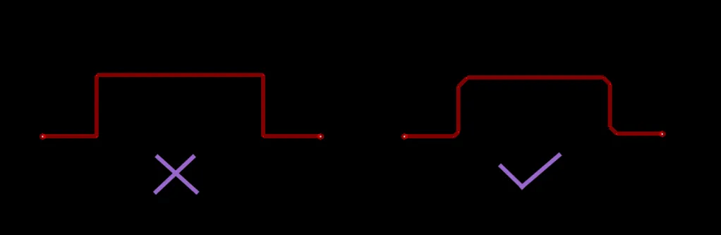
7. No acute or right-angle corners
- A right angle or acute angle adds extra radiation, is harder to fabricate cleanly, and creates an impedance step.
- Use a 45° bend or an arc. That is both a fabrication baseline and an electrical baseline.
Summary
| Point | Rule in one line |
|---|---|
| Routing order | Critical nets → dense regions → ordinary nets |
| Crosstalk | Use 3W, add ground isolation, stay close to the ground plane |
| Layer-to-layer routing | Adjacent layers orthogonal; isolate high-speed layers with a ground plane |
| Signal loop | Smaller loop area, stronger immunity |
| Detail bans | No stubs, no sudden width changes, no self-loops, no right angles |
PCB routing is not only labor. It is sequence, rules, and experience. Random traces still fail after they are drawn. Follow the rules and the first pass is more likely to route cleanly and pass test.