Engineers who have done EMC corrective work have usually seen this: radiated emissions fail, the failing frequencies stay locked, and ferrite beads, filter capacitors, a shield can, and even extra copper pour still leave the same line standing on the spectrum analyzer. Worse, after one peak is finally pushed down, another failing frequency appears next to it. The more the board is changed, the messier the plot becomes.
Most failed EMC campaigns do not fail because too few methods were used. They fail because the noise source was sought in the wrong place. Remedy after remedy is applied, while the real fault stays hidden.
This article walks through one industrial-control board. Radiated emissions stayed over the limit from 200 MHz to 400 MHz. Standard methods all failed. The source was a place many engineers skip: a broken return path when the signal changed layers.
1. The Bind: A Spectrum That Got Worse With Each Change
Where the problem sat
The industrial-control board was a four-layer PCB. Signals ran on the top and bottom layers. The two inner layers were power and ground planes. The main device was an ARM Cortex-M4 running at 168 MHz. The board also had several high-speed SPI interfaces and external SRAM.
During radiated-emission testing, the failures clustered at 200 MHz, 336 MHz, and 400 MHz, by 6 dB to 12 dB. 336 MHz was clearly the second harmonic of 168 MHz. 400 MHz was close to a harmonic of the SRAM clock.
First round: the usual methods
Source filtering came first. A 22 Ω series resistor was added on the SPI clock and SRAM clock lines, with a 10 pF capacitor to ground at the output. After one measurement, 336 MHz dropped about 4 dB but was still over the limit. 200 MHz and 400 MHz barely moved.
Ferrite beads came next. Beads were placed in series on every external interface signal, and one more at the power entry. 200 MHz shifted slightly. 400 MHz rose by 2 dB. At high frequency the bead's parasitic capacitance became a coupling path.
Then shield cans. Metal shields were added over the main device and the SRAM and fixed with conductive adhesive. In principle the cans should have reduced radiation. The measured result did not: the three frequencies dropped only 1 dB to 3 dB, far short of the need.
By this point nearly two weeks had gone by and the design had been through seven or eight revisions. The spectrum still sat above the limit line.
2. Why the Usual Methods All Failed
Limits of filters and beads
Looking back, filter capacitors and beads can attenuate differential-mode noise to some degree. Radiated-emission failures are often not differential-mode radiation. They are common-mode radiation. If the loop area of the common-mode current is large, even a current of only microamperes can radiate enough to fail.
Filtering only suppresses differential-mode noise. It does not improve the path of the common-mode current. More filter parts therefore cannot bring the radiation down while the common-mode loop stays the same.
Why the shield cans did little
A shield can only blocks direct radiation from inside it. If noise has already coupled through inner PCB planes onto traces, or traveled through vias to the board edge, the can cannot stop it. The can addresses radiation from the antenna itself. It does not cut the path that carries noise to that antenna.
The core relationship for radiated emissions is E ∝ I × A × f2, where I is common-mode current, A is loop area, and f is frequency. Filtering changes I, but if loop area A stays the same, the effect is limited. Shrinking A is the root fix.
3. The Hidden Source: A Broken Return Path at the Layer Change
How the problem was found
The turn came during a closer layout review. A near-field probe scanned the board section by section and found unusually strong radiation around several vias in the middle of the board. Those vias were the signal vias where the SPI clock and data lines changed from the top layer to the bottom layer.
The critical fault was this: when the signals left the top layer for the bottom layer, no return ground via had been placed between the adjacent ground and power planes. Return current had to travel around most of the board to reach the new reference plane, and the loop area grew by tens of times.
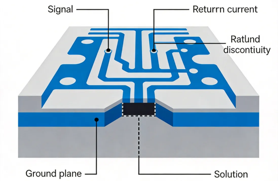
How a return path breaks
While a signal travels, return current follows the lowest-impedance path. On one layer, that current flows in the reference plane directly underneath. The path is compact and the loop area is small.
When the signal changes layers through a via, if the reference also changes from ground to power, or if the ground plane itself has a gap, the return current cannot follow the signal through the layer change. It must detour to another via or a decoupling capacitor to reach the new reference plane. That detour creates a large return area.
From the radiation relationship, once loop area A grows, even a few microamperes of common-mode current can exceed the limit at a few hundred megahertz.
Why this source stays hidden
Several reasons:
Vias are so common on a PCB that almost no one checks whether each via still has a complete return path. DRC reports opens and shorts. It does not flag a discontinuous return path. During near-field scans, attention usually stays on obvious sources such as the IC and the clock generator, and the via neighborhood is easy to skip. The signal itself also functions correctly, with no timing fault, so functional test never shows the problem.
4. The Targeted Fix Started With the Return Path
Add a return ground via next to each signal layer-change via
The direct step: within 50 mil of each signal layer-change via, add a via that ties the two ground planes together—a return ground via. That via gives the return current a low-impedance layer-change path, and the loop area shrinks at once.
On this industrial-control board, one return ground via was added next to each of the six SPI signal layer-change vias. The same was done at the SRAM address and data layer changes. Eighteen return ground vias were added in total.
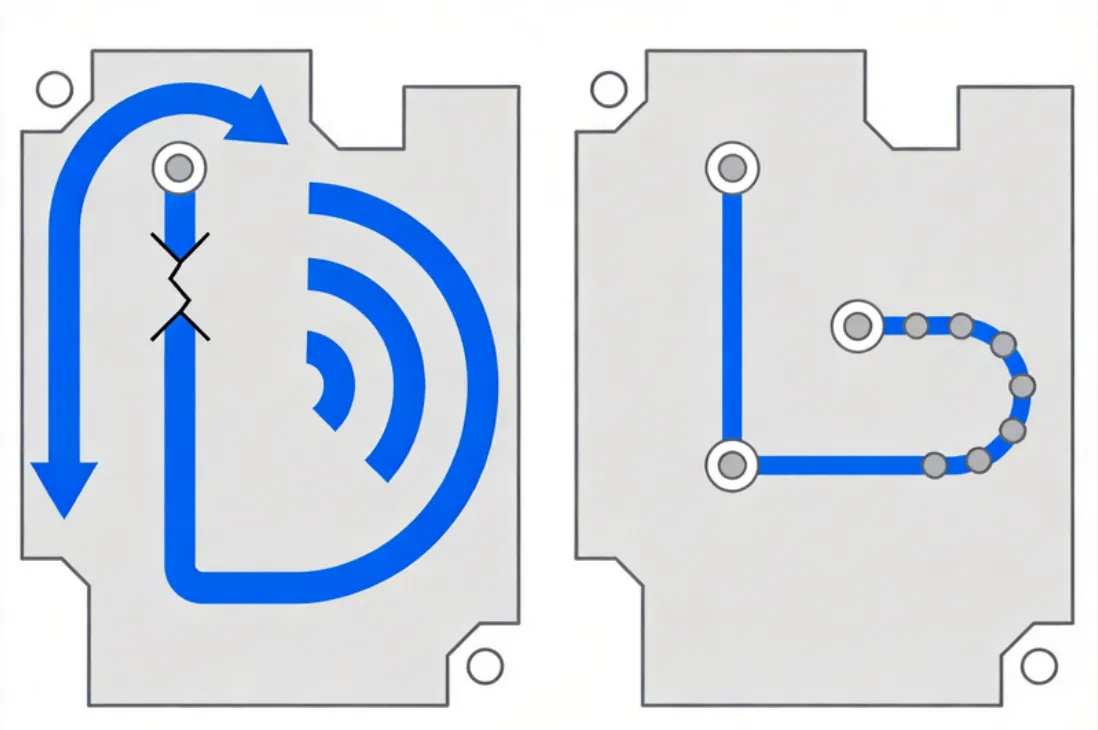
Use decoupling capacitors to help the return
In dense layer-change regions, if the reference switches from a ground plane to a power plane, return current must pass through a decoupling capacitor to get back to ground. Adding 0.1 μF capacitors near those locations opens another return channel. Place each capacitor as close as possible to the layer-change via, within 200 mil.
Restore continuity of the ground plane
A full-board check of the ground plane found four traces occupying ground-plane area and leaving slots. Those slots did not break DC continuity, but to high-frequency return current they acted as a wall and forced a detour. Moving those traces to signal layers restored plane integrity, and the return path opened up.
5. Results and Design Lessons
Test results
After the change, 200 MHz dropped 10 dB, 336 MHz dropped 14 dB, and 400 MHz dropped 8 dB. All three met the limit, with 4 dB to 6 dB of margin. After the return path was fixed, some of the earlier beads and filter capacitors were removed, and signal quality improved. The beads themselves had introduced impedance discontinuities and degraded signal integrity.
Prevention during PCB design
EMC problems are not created in the chamber. They are created in layout. A few habits at design time avoid a large later respin:
- When a signal changes layers, place a return ground via next to the signal via. That is the basic rule.
- Do not let traces split the ground plane. Keep the plane intact.
- Keep high-speed signals on one layer when possible and reduce layer changes.
- If the reference plane changes at the layer change, place a nearby decoupling capacitor to provide a return channel.
- During PCB review, go beyond ordinary DRC and manually check whether the return path of each critical signal stays continuous.
The risk in EMC work is not a shortage of methods. It is working in the wrong direction. When a frequency will not move after repeated filtering and shielding, stop and ask whether the loop area is the problem, and whether the most ordinary via is missing a return ground via beside it.
Finding the real noise source matters more than stacking more corrective parts.