Foundational module circuits appear across almost every electronics project. This article walks through several representative building blocks—regulated power supplies, classic operational amplifier configurations, waveform generators, signal-processing circuits, sensor interfaces, and common display modules—and explains how to read and understand their typical schematics and functional roles in a complete design.
Before diving into each module, consider the example schematics below. If you can interpret these at a glance, you already have a solid start. If not, the following sections will help build that intuition.

Figure 1 | TDA2030 circuit schematic

Figure 2 | 34063 converter circuit

Figure 3 | 555 circuit

Figure 4 | TDA2030 circuit schematic

Figure 5 | Discrete transistor circuit
Regulated DC Power Supplies
A stable DC power supply is the energy backbone of an electronic device. It directly affects system stability and reliability, making it a critical stage in any design. Typical implementation paths include three-terminal fixed (positive or negative) linear regulators, three-terminal adjustable (positive or negative) regulators, and DC-DC converter circuits. Each category has characteristic application circuits and layout considerations.
The rectifier stage converts an AC input U1 into a pulsating DC U2. Common rectification schemes include half-wave and full-wave. A diode bridge can be used to implement full-wave rectification. Typical rectifier diodes include IN4007 and IN5148, while integrated bridge rectifiers such as RS210 are also widely used.
The filter stage smooths the pulsating DC U2 to produce a lower-ripple output U3. Classical options include RC filters, KL filters, and π-type filters. In many low-power designs, an RC filter is a practical and common choice. Selecting the filter topology and component values depends on allowed ripple, load current, and line frequency.
In practical regulator application circuits, both the regulator input and output pins typically use bulk capacitors to ground for energy storage. In addition, small decoupling capacitors Ci and Co (on the order of 0.1 μF to 10 μF) should be placed close to the regulator pins. Ci helps suppress self-oscillation by stabilizing the regulator’s input, while Co helps limit the high-frequency bandwidth at the output, reducing high-frequency noise. Appropriate values depend on the regulator’s output voltage, load dynamics, and the surrounding circuit topology. Placement and parasitics (ESR/ESL) are also important to ensure stability.

Figure 6 | Basic application circuit for a 78-series three-terminal regulator
Operational Amplifiers: Types, Parameters, and Classic Topologies
Operational amplifiers (op-amps) come in many categories to suit different applications, including general-purpose, precision, low-noise, high-speed, low-voltage/low-power, and single-supply types. Selecting an op-amp involves balancing a set of parameters against system targets and constraints.
Key performance parameters include: single/dual supply operating voltage, quiescent supply current, input offset voltage, input offset current, input resistance, slew rate, differential-mode input resistance, offset current temperature drift, input bias current and its temperature drift, differential voltage gain, common-mode voltage gain, unity-gain bandwidth, power-supply rejection, differential-mode input voltage range, common-mode input voltage range, input-referred noise voltage, input-referred noise current, offset voltage temperature drift, settling time, and long-term drift.

Figure 7 | Non-inverting proportional amplifier

Figure 8 | Differential amplifier
Waveform Generation
Generating waveforms such as square waves, sine waves, triangle waves, and single pulses is a frequent requirement in development and testing. Practical implementations often use op-amps or dedicated analog ICs with a few external components to form oscillators and waveform-shaping networks. The choice of topology depends on the desired waveform quality, frequency range, amplitude stability, and component availability.
Figure 9 | Rectangular wave generator using discrete analog circuitry

Figure 10 | Self-excited equivalent-inductance oscillator
Signal Processing Circuits
Signal conditioning functions can be quickly realized using op-amps or dedicated analog ICs with a small number of passives. Typical functions include signal amplification, filtering, impedance matching, level shifting, non-linear compensation, current-to-voltage (I/V) conversion, and voltage-to-frequency (V/F) conversion. Proper selection of topology, order, and component values allows a designer to meet bandwidth, noise, and linearity requirements without excessive complexity.

Figure 11 | Active low-pass filter using an op-amp

Figure 12 | Audio alarm circuit
Sensor Basics and Interface Examples
A sensor responds to a specified physical quantity (the measurand) and converts it into a usable electrical signal according to a defined relationship. A typical sensor system comprises a sensing element that directly responds to the measurand, a transduction element that produces an electrical output, and supporting electronics for biasing, amplification, filtering, linearization, and output scaling.

Figure 13 | Basic Hall-effect sensor application

Figure 14 | Photoelectric detection circuit
Displays: LED and LCD Modules
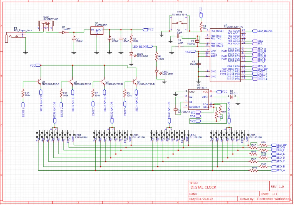
LED displays, composed of light-emitting diodes, are among the most common visual indicators. A seven-segment LED display uses seven segments to form digits and is often referred to as a seven-segment display or “numeric tube.” Many devices include an additional dot LED for decimal-point indication. Driving a seven-segment LED typically involves current-limiting resistors, multiplexing (for multi-digit displays), and proper pin mapping for common-anode or common-cathode variants.
LCDs operate by reorienting rod-like liquid crystal molecules with an applied electric field. Because these molecules have dipole moments, their alignment affects the polarization of transmitted light. By modulating this alignment, an LCD can present bright/dark or transmissive/non-transmissive states to form characters or graphics. In practice, driving a dot-matrix character LCD module (MDLS) involves generating proper control signals, timing, and data sequences. Hardware such as an FPGA can be used to orchestrate address scanning, character data output, and display refresh.

Figure 15 | Block diagram of an LCD module circuit
Together, these module circuits form the essential toolkit for modern electronics. Mastering their schematics and understanding how each block functions—power conversion and regulation, op-amp configurations, waveform generation, signal conditioning, sensing, and display driving—enables robust system design and faster, more confident development.